Piezoelectric MEMS switch and method of manufacturing piezoelectric MEMS switch

a technology of piezoelectric and mems switches, which is applied in the field of micro electro mechanical system (mems) switches, can solve the problems of not being able prone to sticking phenomena in the attracted contact portion, and being unable to follow high-speed on/off driving in a high-frequency range. , to achieve the effect of improving the reliability of switching on and off operations, reducing warping of dia

Inactive Publication Date: 2011-06-23
FUJIFILM CORP
View PDF3 Cites 19 Cited by
  • Summary
  • Abstract
  • Description
  • Claims
  • Application Information

AI Technical Summary

Benefits of technology

[0040]According to this aspect of the invention, it is possible to reduce warping of the diaphragm in the manufacturing stage, and the reliability of the switching on and off operations is improved.
[0041]According to the present invention, by using a piezoelectric drive method as a drive source for performing contacting and separating operations of a switch contact, and adopting a composition in which piezoelectric drive sections are provided on both the front and rear surfaces of a diaphragm, it is possible to achieve better high-frequency response (tracking: following capability) compared to a conventional electrostatic method, and it is also possible to exert a strong drive force in the return direction of the diaphragm (mem

Problems solved by technology

In the case of a switching operation by attraction or repulsion due to electrostatic force, it becomes impossible to follow high-speed on/off driving in a high-frequency range, due to accumulation of charge in the piezoelectric bodies which are adjacent to the electrodes.
Further, there is a possibility of not being able to follow high-speed on/off driving in a high-frequency range due to dielectric loss of the adjacent piezoelectric bodies in the high-frequency range.
In this case, a sticking phenomenon is liable to occur in the attracted contact portion.
In the case of miniature devices such as mobile devices in particular, the circuitry of the drive system must be kept simple, but with a related-art electrostatic drive system, it has been necessary to raise the drive voltage and therefore power consumption has become large.
Moreover, the drive circuit in a case of a driving operation by attraction and repulsion based on electrostatic force is required to correspond to both positive and negative voltage drivings, and the extent to which costs and circuit size can be reduced is limited because a drive circuit such

Method used


Image

  • Piezoelectric MEMS switch and method of manufacturing piezoelectric MEMS switch
  • Piezoelectric MEMS switch and method of manufacturing piezoelectric MEMS switch
  • Piezoelectric MEMS switch and method of manufacturing piezoelectric MEMS switch

Examples


modification examples

Further Modification Examples

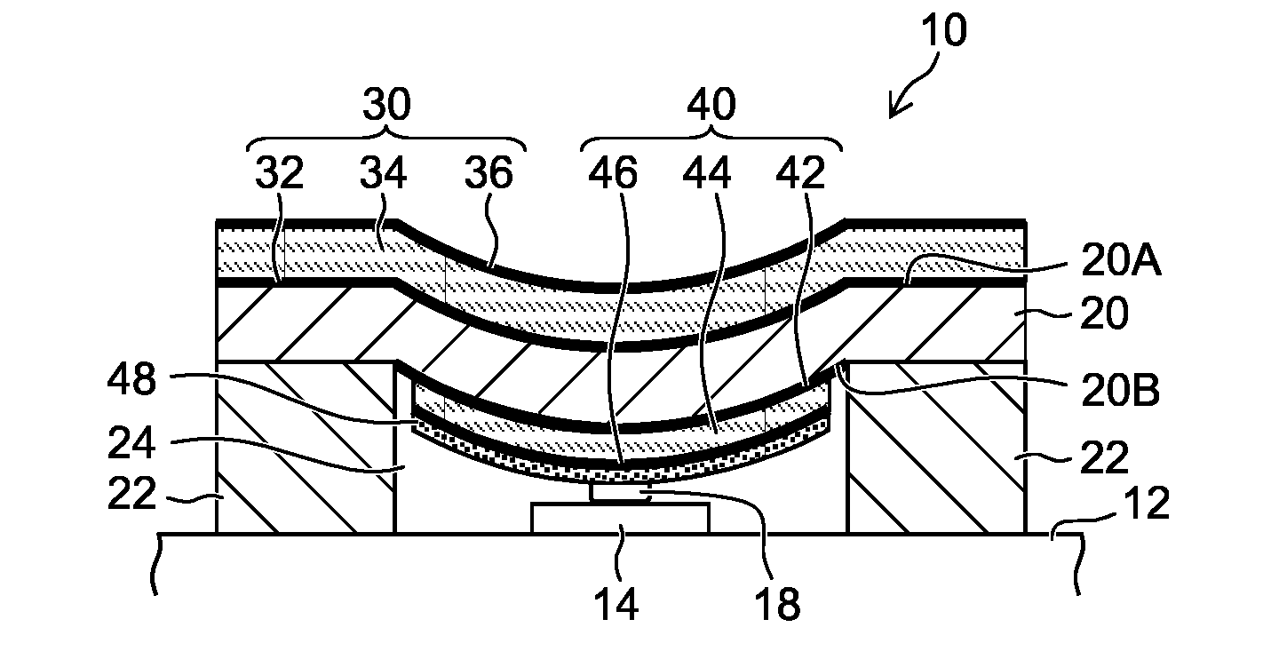
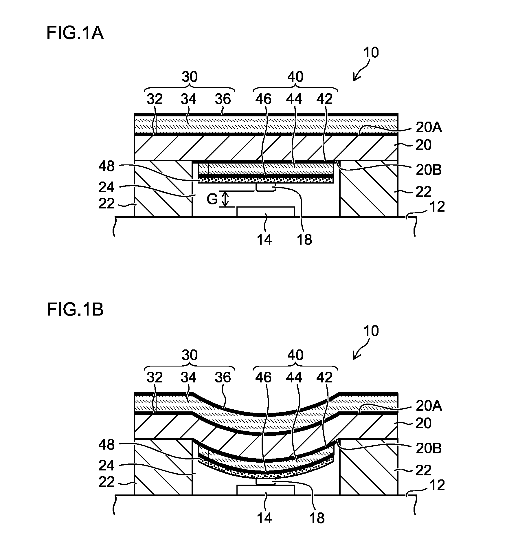
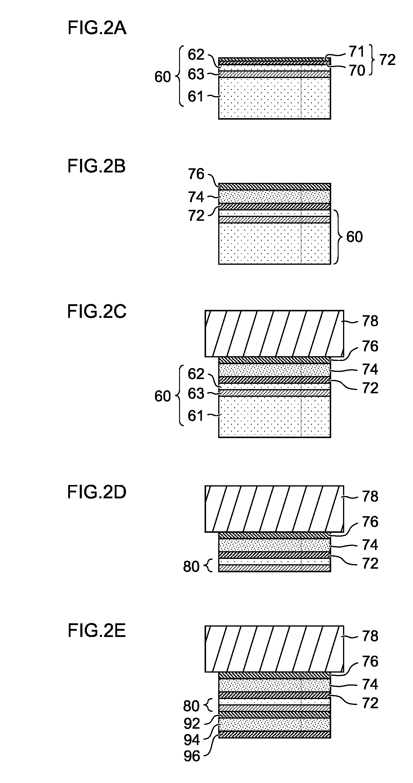
[0106]The implementation of embodiments of the present invention is not limited to the piezoelectric body material, electrode material, film forming conditions, film thickness dimensions, drive voltage, and other conditions stated in the first practical example shown in FIGS. 2A to 4C and the second practical example shown in FIGS. 7A to 7D, but rather an embodiment of the present invention can be implemented under various conditions.

[0107]Moreover, in the embodiments described above, a structure is described in which a movable electrode 18 makes contact with one fixed electrode 14, but in implementing an embodiment of the present invention, it is also possible to adopt a switch structure in which a plurality of fixed electrodes (for example, a first fixed electrode and a second fixed electrode) are arranged on a base substrate, an electrical connection is established between the plurality of fixed electrodes (switch on) by means of a movable electrode m...


PUM

PropertyMeasurementUnit
Thicknessaaaaaaaaaa
Electric potential / voltageaaaaaaaaaa
Piezoelectricityaaaaaaaaaa

Abstract

A piezoelectric MEMS switch includes: a base substrate; a diaphragm arranged to oppose the base substrate via a gap; a first piezoelectric drive section constituted by layering a first lower electrode, a first piezoelectric body and a first upper electrode on a first surface of the diaphragm, the first surface being across the diaphragm from the gap; a second piezoelectric drive section constituted by layering a second lower electrode, a second piezoelectric body and a second upper electrode on a second surface of the diaphragm, the second surface facing the gap; a fixed electrode provided on a gap side of the base substrate; and a movable electrode which is fixed to a second piezoelectric drive section side of the diaphragm and opposes the fixed electrode in such a manner that the movable electrode makes contact with and separates from the fixed electrode according to displacement of the diaphragm.

Description

BACKGROUND OF THE INVENTION[0001]1. Field of the Invention[0002]The present invention relates to a micro electro mechanical system (MEMS) switch, and more particularly to a MEMS switch having a piezoelectric drive system using a piezoelectric body thin film, and to a method of manufacturing same.[0003]2. Description of the Related Art[0004]In recent years, there has been extensive research and development of micro electro mechanism systems (MEMS) applied to semiconductor manufacturing processes, and switch structures of various types have been proposed in the field of MEMS switches, which is one example of the application of MEMS technology (see, for example, International Publication No. WO 2004 / 019362 A1 and Japanese Patent Application Publication No. 2007-157511).[0005]International Publication No. WO 2004 / 019362 A1 proposes a structure in which a plurality of actuator fingers having alternately arranged positive and negative electrodes are provided as a drive source on a surface...

Claims


Application Information

Patent Timeline
IPC IPC(8): H01H57/00H01L41/22B81B3/00B81C1/00H01H49/00H01L41/09H01L41/314
CPCH01H57/00H01H2057/006Y10T29/42H01L41/0973H01L41/0926H10N30/2047H10N30/204
Inventor NIHEI, YASUKAZU
Owner FUJIFILM CORP
Why Eureka
Try Eureka