Nanowire Solar Cell and Manufacturing Method of the Same

a solar cell and nanowire technology, applied in the field of nanowire solar cells, can solve the problems of inability to obtain sufficient photoelectric conversion efficiency, inability to manufacture devices capable of generating practical electric power, temperature cannot be raised, etc., to achieve the effect of preventing recombination of excitons, preventing contamination, and improving photoelectric conversion efficiency

Inactive Publication Date: 2011-06-30
HONDA MOTOR CO LTD +1
View PDF7 Cites 13 Cited by
  • Summary
  • Abstract
  • Description
  • Claims
  • Application Information

AI Technical Summary

Benefits of technology

[0017]An object of the present invention is to eliminate such disadvantages, to provide a solar cell which is capable of configuring a device with a plurality of nanowire semiconductors arranged in an array form, and which is capable of obtaining practical electric power and effectively collecting excitons, and to provide a manufacturing method of the solar cell.
[0018]To this end, the present invention provides a nanowire solar cell which includes a semiconductor substrate and a plurality of nanowire semiconductors grown on the semiconductor substrate to form pn junctions, and which is featured by comprising: a transparent insulating material filled in the gap between the plurality of nanowire semiconductors; an electrode which is continuously provided on the transparent insulating material to cover the end portion of the plurality of nanowire semiconductors, the end portion being opposite to the semiconductor substrate, and is connected to the plurality of nanowire semiconductors; and a passivation layer which is provided, along the surface of the plurality of nanowire semiconductors, between the plurality of nanowire semiconductors and the transparent insulating material and between the plurality of nanowire semiconductors and the electrode, so as to prevent recombination of excitons.
[0019]In the nanowire solar cell having the above described configuration according to the present invention, the area of the contact interface between the nanowire semiconductors and the electrode connected to the nanowire semiconductors can be reduced by the provision of the transparent insulating material, to thereby reduce the number of defects caused on a current path by a photovoltaic force. As a result, the recombination sites resulting from the defects in the boundary surface can be easily saturated, so that the photoelectric conversion efficiency can be improved and practical electric power can be obtained.

Problems solved by technology

Thus, there is a problem that a device capable of generating practical electric power cannot be manufactured with the nanowire solar cell.
Further, the nanowire solar cell has a problem that, when the i-type Si semiconductor layer and the n-type Si semiconductor layer are formed as the shell layers, the temperature cannot be raised until the layers are epitaxially grown, and hence the i-type Si semiconductor layer and the n-type Si semiconductor layer are polycrystallized.
The problem is due to the fact that, when the temperature is raised by heating to the epitaxial growth temperature, the catalyst metal is thoroughly incorporated into the nanowire of the p-type Si semiconductor layer serving as the core of the core shell structure.
Since a plurality of dangling bonds existing in the crystal grain boundaries promote recombination of excitons, the sufficient photoelectric conversion efficiency cannot be obtained.
However, in the nanowire solar cell, since the lower contact is formed after the nanowire of p-type Si semiconductor is formed by using the pore of the template layer, the lower contact is limited to a metal contact or a transparent electrode, and single-crystal semiconductor material cannot be used for the lower contact.
However, in the nanowire solar cell, the lower contact made of a planar single crystal semiconductor cannot be formed by the epitaxial growth process after the formation of the nanowire.
Further, there is a problem that, according to the VLS method, the metal material remains in the boundary surface between the substrate and the nanowire.
However, there is no guarantee that, when the crystal of the substrate and the crystal the nanowire are connected to each other, their orientation is maintained.
However, as described above, the VLS method has a problem that the metal catalyst remains at both ends of the nanowire.
Further, in any of the above described solar cells, it is not possible to obtain practical electric power.

Method used


Image

  • Nanowire Solar Cell and Manufacturing Method of the Same
  • Nanowire Solar Cell and Manufacturing Method of the Same
  • Nanowire Solar Cell and Manufacturing Method of the Same

Examples


Embodiment Construction

[0030]Next, an embodiment according to the present invention will be described with reference to the accompanying drawings.

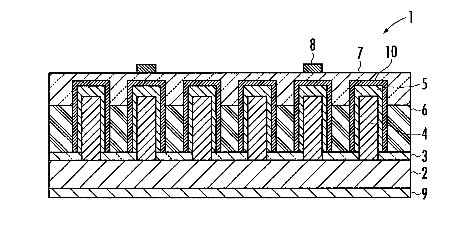
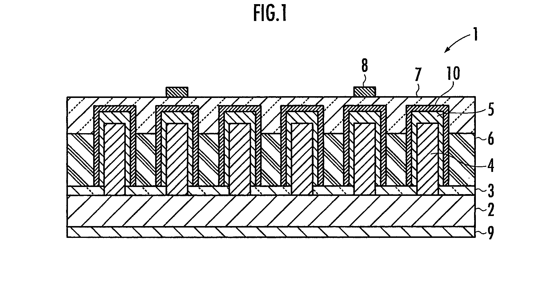
[0031]First, a nanowire solar cell 1 of a present embodiment will be described with reference to FIG. 1. The nanowire solar cell 1 comprises an amorphous SiO2 coating 3 formed on an InP (111) A substrate 2, and a nanowire p-type InP semiconductor 4 formed on the InP (111) A substrate 2 exposed from the amorphous SiO2 coating 3. The nanowire p-type InP semiconductor 4 comprises an n-type InP semiconductor 5 along the surface shape thereof, and an i-type InP semiconductor (not shown) is provided between the p-type InP semiconductor 4 and the n-type InP semiconductor 5. Here, the nanowire solar cell 1 has a core shell structure in which the p-type InP semiconductor 4 is used as the core and in which the i-type InP semiconductor and the n-type InP semiconductor 5 are used as the shell.

[0032]The nanowire solar cell 1 comprises a transparent insulating material 6 fill...


PUM

PropertyMeasurementUnit
Vocaaaaaaaaaa
transparentaaaaaaaaaa
semiconductoraaaaaaaaaa

Abstract

To provide a solar cell enabling practical electric power to be obtained and excitons to be effectively collected, and a manufacturing method of the solar cell. A nanowire solar cell 1 comprises: a semiconductor substrate 2; a plurality of nanowire semiconductors 4 and 5 forming pn junctions; a transparent insulating material 6 filled in the gap between the plurality of nanowire semiconductors 4 and 5; an electrode 7 covering the end portion of the plurality of nanowire semiconductors 4 and 5; and a passivation layer 10 provided between the semiconductor 5 and the transparent insulating material 6 and between the semiconductor 5 and the electrode 7.

Description

CROSS-REFERENCE TO RELATED APPLICATION[0001]This application is based upon and claims the benefit of priority from Japanese Patent Application No. 2009-295806 filed on Dec. 25, 2009, of which the contents are incorporated herein by reference.BACKGROUND OF THE INVENTION[0002]1. Field of the Invention[0003]The present invention relates to a nanowire solar cell comprising nanowire semiconductors, and a manufacturing method of the nanowire solar cell.[0004]2. Description of the Related Art[0005]Generally, a solar cell is known in which a planar pn junction surface is provided in parallel with the substrate surface. In recent years, a solar cell (hereinafter referred to as nanowire solar cell) comprising a fine linear semiconductor having a nano order diameter and referred to as a nanowire, a nanorod, and the like, is known in addition to the conventional common solar cell.[0006]Further, in the nanowire solar cell, a technique is proposed in which the photoelectric conversion efficiency ...

Claims


Application Information

Patent Timeline
Patent Type & Authority Applications(United States)
IPC IPC(8): H01L31/06H01L31/0352B82Y40/00H01L31/0216H01L31/0735
CPCH01L31/02167H01L31/035227H01L31/03529Y02E10/544H01L31/077H01L31/184H01L31/0693Y02E10/547Y02P70/50
Inventor GOTO, HAJIMEFUKUI, TAKASHIMOTOHISA, JUNICHIHIRUMA, KENJI
Owner HONDA MOTOR CO LTD
Why Eureka
Try Eureka