Solid-state imaging device, method of manufacturing the same, and electronic apparatus

Active Publication Date: 2011-06-30
SONY CORP
View PDF2 Cites 83 Cited by
  • Summary
  • Abstract
  • Description
  • Claims
  • Application Information

AI Technical Summary

Benefits of technology

[0014]The present invention provides a solid-state imaging device with improved transfer efficiency without impeding miniaturization of a pixel, and a method of manufacturing the same, in a solid-state imaging de

Problems solved by technology

Therefore, sensitivity or an S/N ratio deteriorates.
Therefore, in the red pixel, since green and blue lights are used for photoelectric conversion, loss occurs in light use efficiency.
In addition, since the interpolation process is not performed, false colors are not generated.
Therefore, dark current due to the PN junction with the high electric field causes noise.
Then, linearity of an out

Method used


Image

  • Solid-state imaging device, method of manufacturing the same, and electronic apparatus
  • Solid-state imaging device, method of manufacturing the same, and electronic apparatus
  • Solid-state imaging device, method of manufacturing the same, and electronic apparatus

Examples


first embodiment

Solid-State Imaging Device

[0064]First, a CMOS-type solid-state imaging device 1 as a first embodiment of the present invention will be described with reference to FIG. 1. The configuration of FIG. 1 according to the following embodiments is commonly used in solid-state imaging devices. In the present embodiment, a back irradiation type CMOS type solid-state imaging device 1 is described.

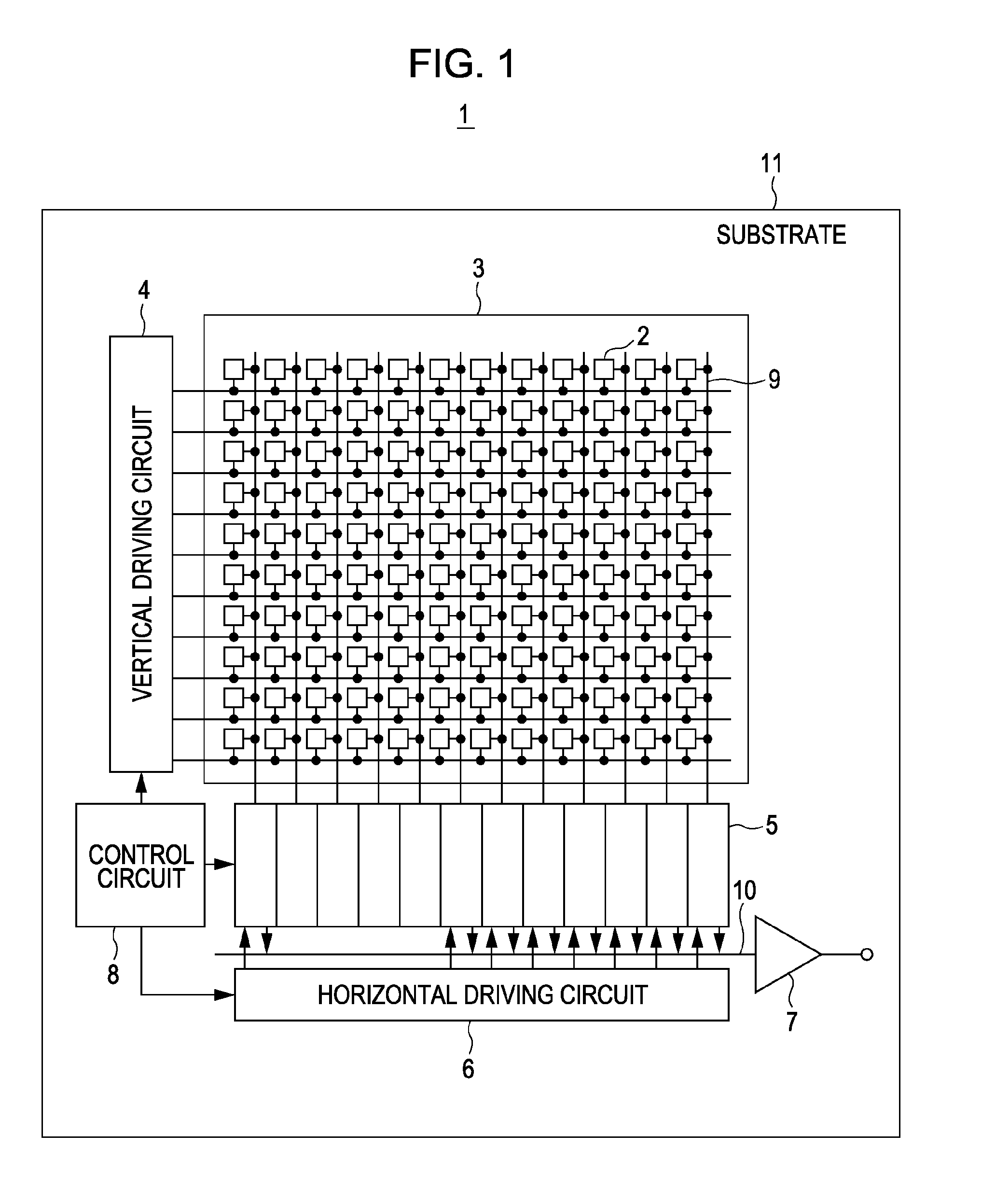
[0065]FIG. 1 is a schematic diagram showing one configuration of a CMOS-type solid-state imaging device 1.

[0066]The solid-state imaging device 1 of the present embodiment includes a pixel region 3 in which a plurality of pixels 2 is arranged on a substrate 11 formed of silicon, a vertical driving circuit 4, column signal processing circuits 5, a horizontal driving circuit 6, an output circuit 7, a control circuit 8, and the like.

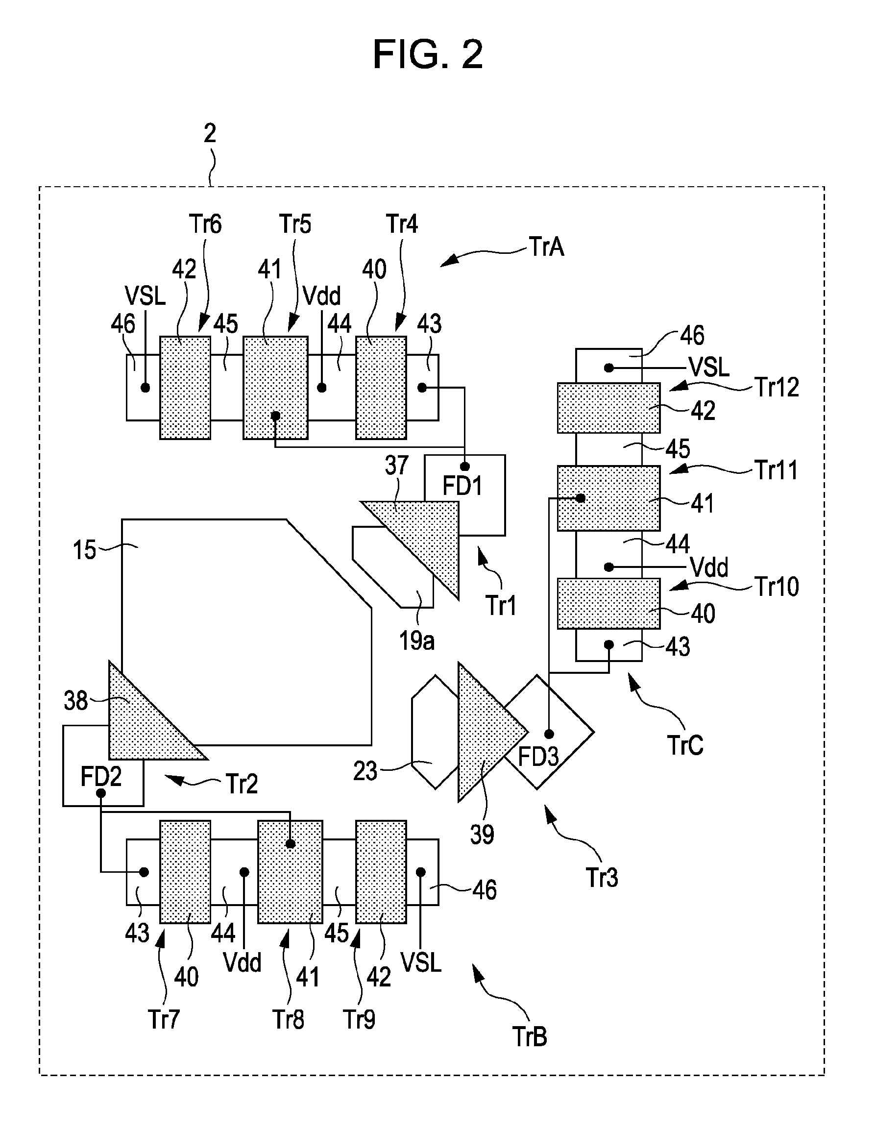
[0067]Each pixel 2 includes a photodiode which is a photoelectric conversion element and a plurality of pixel transistors and a plurality of pixels is regularly arranged on t...

second embodiment

Method of Manufacturing Solid-State Imaging Device

[0133]Next, a method of manufacturing a solid-state imaging device as a second embodiment of the present invention will be described. FIGS. 10A and 10B to 13A and 13B are diagrams showing a process of manufacturing the solid-state imaging device of this embodiment. The solid-state imaging device completed in this embodiment is equal to the solid-state imaging device shown in FIG. 3 and the description thereof will be omitted. In FIGS. 10A and 10B to 13A and 13B, portions corresponding to FIGS. 5A, 5B and 5C to 8A and 8B are denoted by the same reference numerals and the description thereof will be omitted.

[0134]First, as shown in FIG. 10A, an SOI substrate obtained by sequentially forming a BOX layer 52 and a semiconductor layer 17 formed of silicon on a substrate 51 formed of silicon is prepared. This semiconductor layer 17 corresponds to the semiconductor substrate 17 of FIG. 3. The semiconductor layer 17 of the SOI substrate is a ...

third embodiment

Solid-State Imaging Device

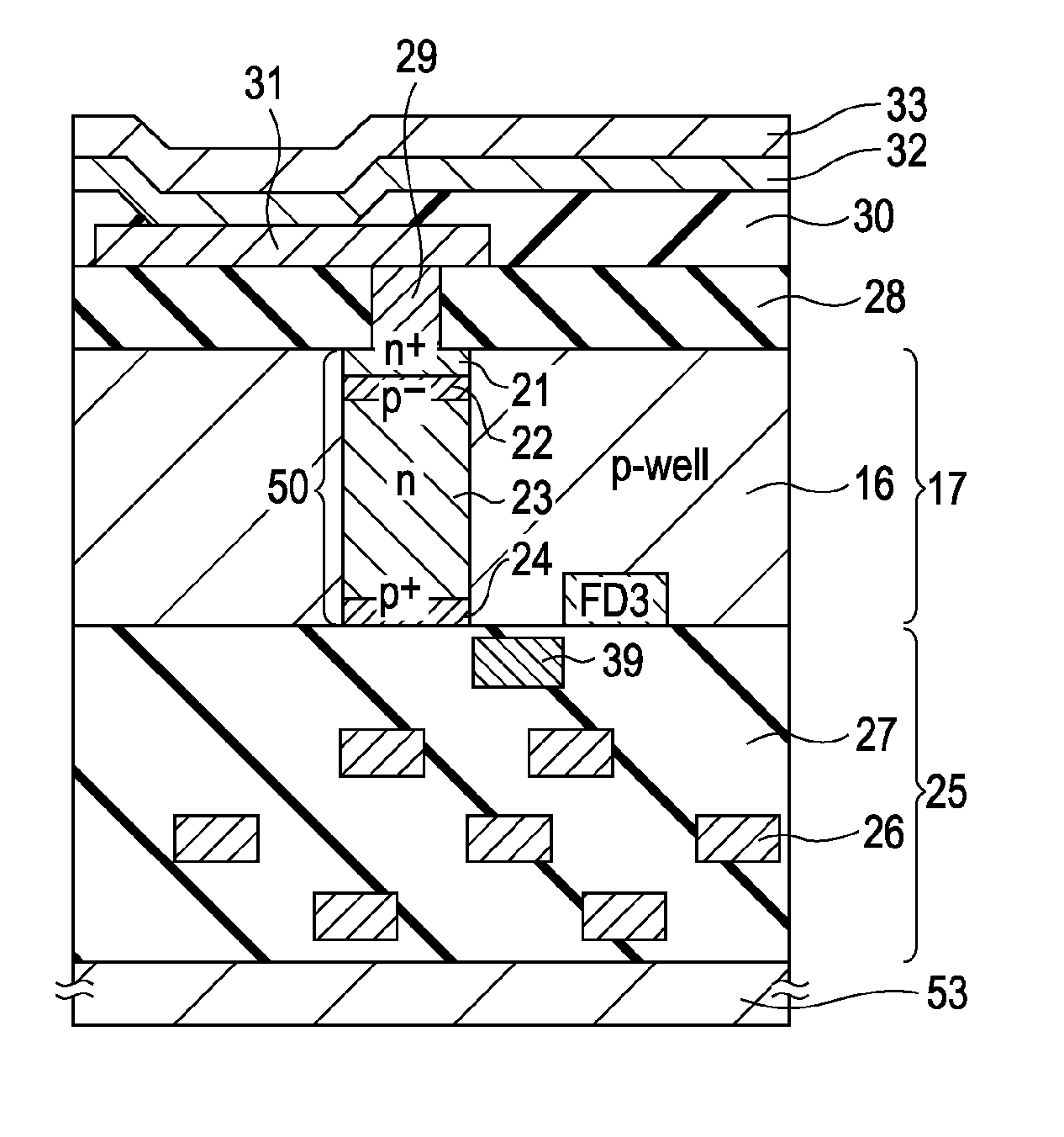
[0143]Next, a solid-state imaging device according to a third embodiment of the present invention will be described. The solid-state imaging device of this embodiment is an example in which a desired transfer transistor of the solid-state imaging device of the first embodiment is set to a vertical type transistor.

[0144]FIG. 14 is a schematic cross-sectional view of the main portions of the solid-state imaging device of this embodiment. In FIG. 14, portions corresponding to FIG. 3 are denoted by the same reference numerals and the description thereof will be omitted.

[0145]In this embodiment, the first photodiode PD1 formed on the light sensing surface side of the semiconductor substrate 17 includes an n-type semiconductor region 60 formed on the rear surface side of the semiconductor substrate 17 and a p-type semiconductor region 61 formed on the front surface side of the semiconductor substrate 17 in contact with the n-type semiconductor region 60. That is,...


PUM


Abstract

A solid-state imaging device including a semiconductor substrate, a photoelectric conversion portion interposed between a lower electrode and an upper electrode, a contact plug formed so as to connect the lower electrode and the semiconductor substrate in order to read signal charges generated in the photoelectric conversion portion to the semiconductor substrate side, a vertical type transmitting path configured by sequentially laminating a connection portion for electrically connecting the contact plug to the semiconductor substrate, a charge accumulation layer for accumulating the signal charges read to the connection portion, and a potential barrier layer configuring a potential barrier between the connection portion and the charge accumulation layer in a vertical direction of the semiconductor substrate, and a charge reading portion configured to read the signal charges accumulated in the charge accumulation layer to the circuit forming surface side of the semiconductor substrate.

Description

RELATED APPLICATION DATA[0001]The present application claims priority to Japanese Priority Patent Application JP 2009-297930 filed in the Japan Patent Office on Dec. 28, 2009, which is incorporated herein by reference in its entirety.BACKGROUND OF THE INVENTION[0002]The present invention relates to a solid-state imaging device such as a CMOS image sensor or a CCD image sensor including a photoelectric conversion unit in which a plurality of pixels is arranged, and, more particularly, to a back irradiation type solid-state imaging device in which a signal circuit is formed on one surface of a substrate so as to receive light from the other surface of the substrate, a method of manufacturing the solid-state imaging device, and an electronic apparatus using the solid-state imaging device.[0003]In recent CCD type or CMOS type image sensors, the number of photons incident to a unit pixel is reduced with reduction of a pixel size. Therefore, sensitivity or an S / N ratio deteriorates. In th...

Claims


Application Information

Patent Timeline
IPC IPC(8): H01L31/113H01L31/18
CPCH01L27/14603H01L27/1464H01L27/14643H01L27/14636
Inventor YAMAGUCHI, TETSUJI
Owner SONY CORP
Why Eureka
Try Eureka