

Acoustic wave device
- Summary
- Abstract
- Description
- Claims
- Application Information
AI Technical Summary
Benefits of technology
Problems solved by technology
Method used
Image

Examples
first preferred embodiment
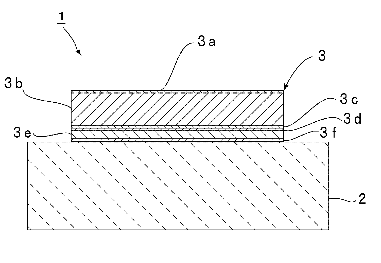
[0026]FIG. 1A is a fragmentary front sectional view of an acoustic wave device 1 according to a first preferred embodiment of the present invention. FIG. 1B is a plan view illustrating the electrode structure of the acoustic wave device 1.
[0027]The acoustic wave device 1 is a surface acoustic wave device that utilizes surface acoustic waves.
[0028]The acoustic wave device 1 includes a piezoelectric substrate 2 and an IDT electrode 3 disposed on the piezoelectric substrate 2. In this preferred embodiment, the piezoelectric substrate 2 is preferably made of LiNbO3, for example. The piezoelectric substrate 2 may be made from a single crystal of a piezoelectric material, such as LiTaO3 or quartz, for example. Alternatively, the piezoelectric substrate 2 may be made of a piezoelectric ceramic, such as lead zirconate titanate (PZT), for example.
[0029]With reference to FIG. 1B, a first reflector 4 and a second reflector 5 are arranged on both sides of the IDT electrode 3 in the propagation ...
second preferred embodiment
[0043]FIG. 5 is a fragmentary front sectional view of an acoustic wave device 21 according to a second preferred embodiment of the present invention.
[0044]The acoustic wave device 21 is preferably a surface acoustic wave device that utilizes surface acoustic waves. The acoustic wave device 21 includes a piezoelectric substrate 22 preferably made of LiNbO3, for example, and an IDT electrode 23 disposed on the piezoelectric substrate 22. Reflectors are arranged on both sides of the IDT electrode 23 in the propagation direction of a surface acoustic wave. An electrode structure including the IDT electrode 23 and the reflectors is substantially the same as described with respect to the acoustic wave device 1 shown in FIG. 1B.
[0045]Preferably, the IDT electrode 23 and the reflectors each include a metal laminate including a plurality of stacked metal layers. The metal laminate preferably has substantially the same configuration as that described for the IDT electrode 3. In the metal lami...
example 1
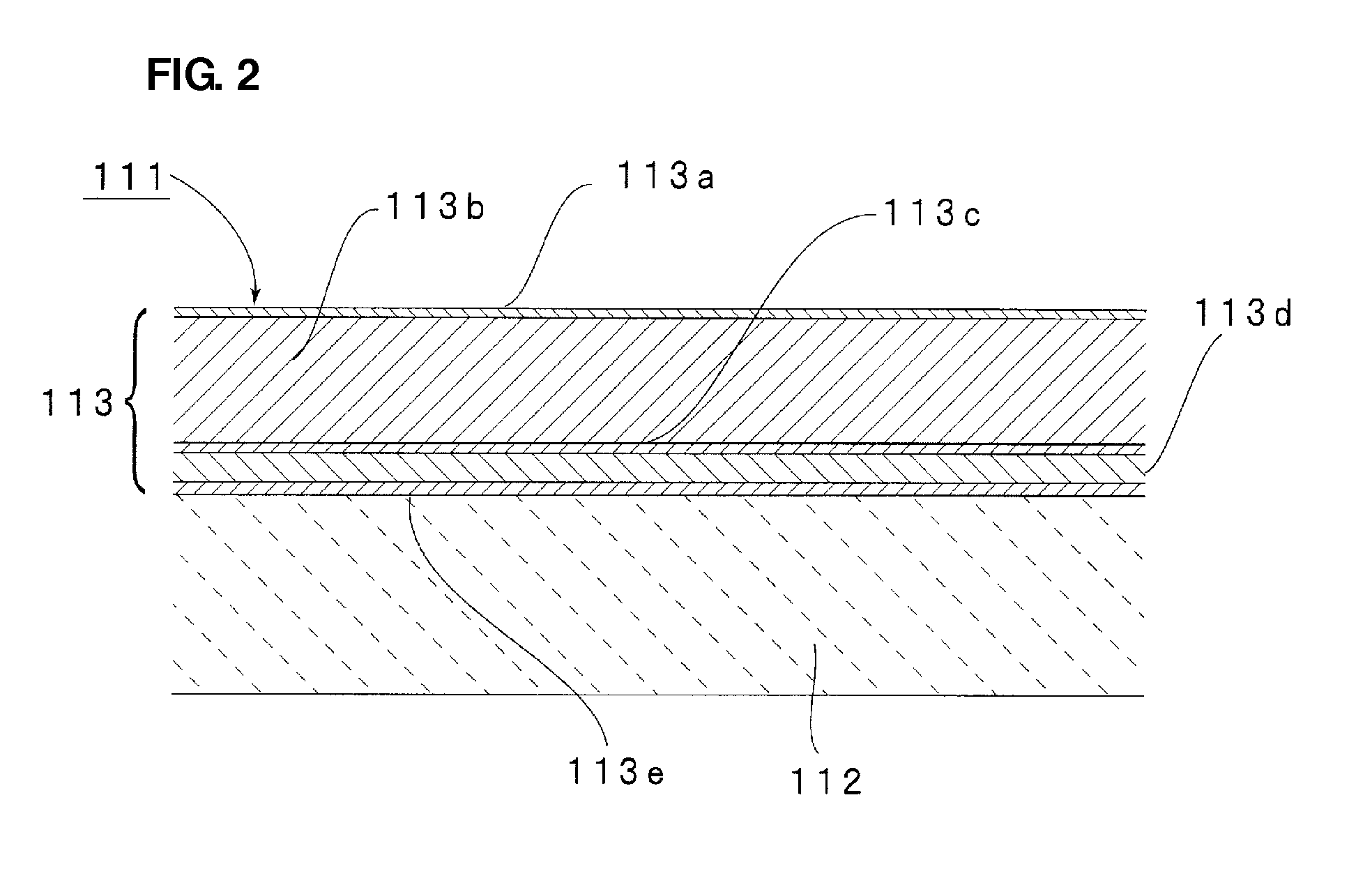
[0058]For the purpose of identifying the effect of preventing interdiffusion, multilayer structures corresponding to the acoustic wave device 1 according to the first preferred embodiment were prepared in substantially the same manner as that described in the first preferred embodiment, except that no IDT electrode was formed but a metal laminate was formed over the upper surface of a LiNbO3 substrate 12 defining a piezoelectric substrate as shown in FIG. 3. In the metal laminate, the following layers were arranged in this order from the top: an upper Ti layer 13a, a first metal layer 13b made of the Al-based alloy described in the first preferred embodiment, a Cu layer 13c, a lower Ti layer 13d, a second metal layer 13e made of Pt, and a Ni—Cr layer 13f. These layers were each substantially identical in thickness to a corresponding one of those described in the first preferred embodiment. In the formation of the metal laminate, these layers were formed on the LiNbO3 substrate 12 in...
PUM
 Abstract
Description
Claims
Application Information