Optoelectronic device and method of forming the same

Active Publication Date: 2011-06-30
UNITED MICROELECTRONICS CORP
View PDF10 Cites 1 Cited by
  • Summary
  • Abstract
  • Description
  • Claims
  • Application Information

AI Technical Summary

Benefits of technology

[0031]As described above, in an optoelectronic device provided by the present invention, an optical waveguide, a coupler, and a MOS device are effectively integrated into a single chip so that less surface area is taken and the system is simplified. In addition, in the me

Problems solved by technology

However, an optoelectronic device fabricated through such a technique takes up too much surface area and has a complicated system.
However, if a MOS devic

Method used


Image

  • Optoelectronic device and method of forming the same
  • Optoelectronic device and method of forming the same
  • Optoelectronic device and method of forming the same

Examples


Embodiment Construction

[0040]Reference will now be made in detail to the present preferred embodiments of the invention, examples of which are illustrated in the accompanying drawings. Wherever possible, the same reference numbers are used in the drawings and the description to refer to the same or like parts.

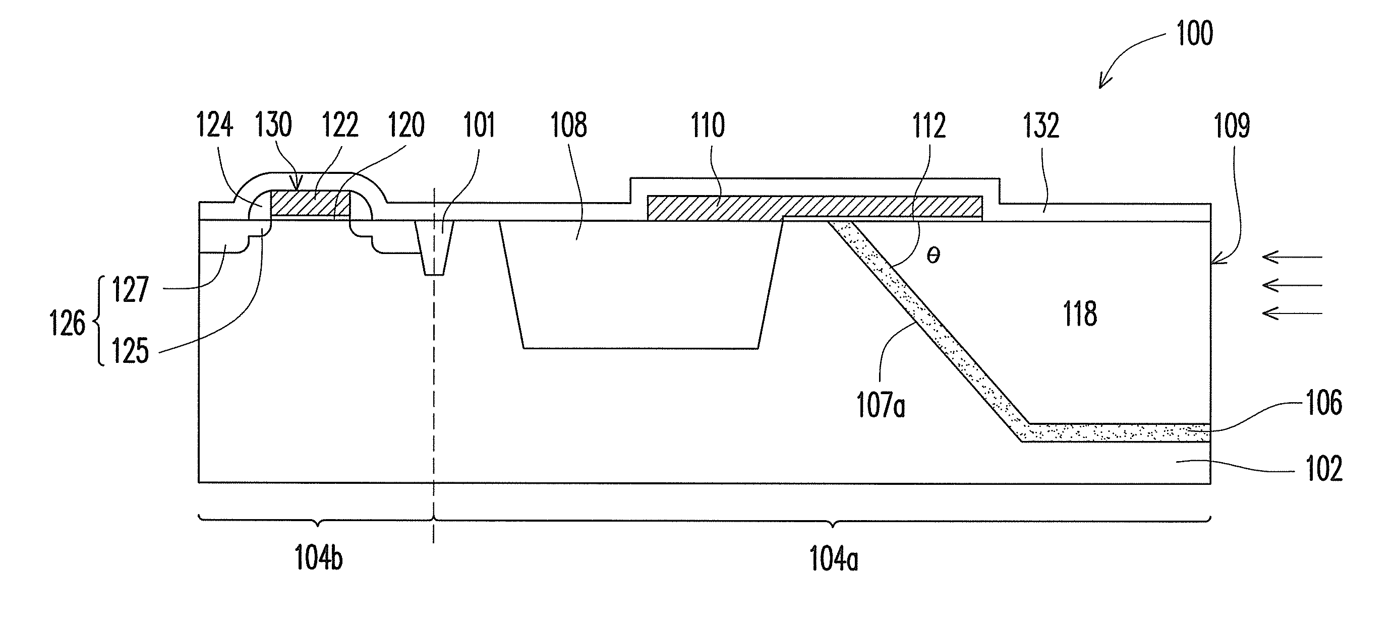
[0041]FIG. 1 is a schematic cross-sectional view of an optoelectronic device according to an embodiment of the present invention.

[0042]Referring to FIG. 1, the optoelectronic device 100 includes a substrate 102, a half-boat-shaped material layer 106, a deep trench isolation structure 108, and an optical waveguide 110. The substrate 102 may be a bulk-Si substrate and has a first area 104a and a second area 104b. The first area 104a is used for forming optical devices (for example, the optical waveguide 110 and a coupler 118), and the second area 104b is used for forming electronic devices (for example, a metal-oxide-semiconductor (MOS) device 130). The first area 104a and the second area 104b may be s...


PUM


Abstract

An optoelectronic device including a substrate, a half-boat-shaped material layer, a deep trench isolation structure, and an optical waveguide is provided. The substrate has a first area. The half-boat-shaped material layer is disposed in the substrate within the first area. The refractive index of the half-boat-shaped material layer is lower than that of the substrate. A top surface of the half-boat-shaped material layer is coplanar with the surface of the substrate. The deep trench isolation structure is disposed in the substrate within the first area and located at one side of a bow portion of the half-boat-shaped material layer. The optical waveguide is disposed on the substrate within the first area. The optical waveguide overlaps a portion of the deep trench isolation structure and at least a portion of the half-boat-shaped material layer.

Description

BACKGROUND OF THE INVENTION[0001]1. Field of the Invention[0002]The present invention generally relates to a semiconductor device and a method of forming the same, and more particularly, to an optoelectronic device and a method of forming the same.[0003]2. Description of Related Art[0004]An optoelectronic device includes both optical devices and electronic devices, wherein the optical devices include a coupler for receiving an optical signal from an optical fiber and an optical waveguide for receiving and transmitting the optical signal, and the electronic devices include a metal-oxide-semiconductor (MOS) device for controlling the optical waveguide. The MOS device controls the optical waveguide to transform the optical signal into an electronic signal so that the optical signal can be used by other electronic devices.[0005]Conventionally, the electronic devices (for example, the MOS device) are formed on a chip while the optical devices (for example, the coupler and the optical wav...

Claims


Application Information

Patent Timeline
IPC IPC(8): G02B6/12H01L21/30
CPCG02B2006/12061G02B6/12004
Inventor SU, TZUNG-IWANG, MING-ILAN, BANG-CHIANGLIAO, TE-KANSU, CHAO-ANHUANG, CHIEN-HSINWU, HUI-MINTAN, TZUNG-HANCHEN, MINLIN, MENG-JIA
Owner UNITED MICROELECTRONICS CORP
Why Eureka
Try Eureka