The trend for the device having multilayered interconnections in smaller circuits generally widens the width of steps due to the surface irregularities on lower interconnection layers, resulting in degradation of flatness.
An increase in the number of interconnection layers could worsen a quality of
film coating (step coverage) over stepped configurations in the process of forming thin films.
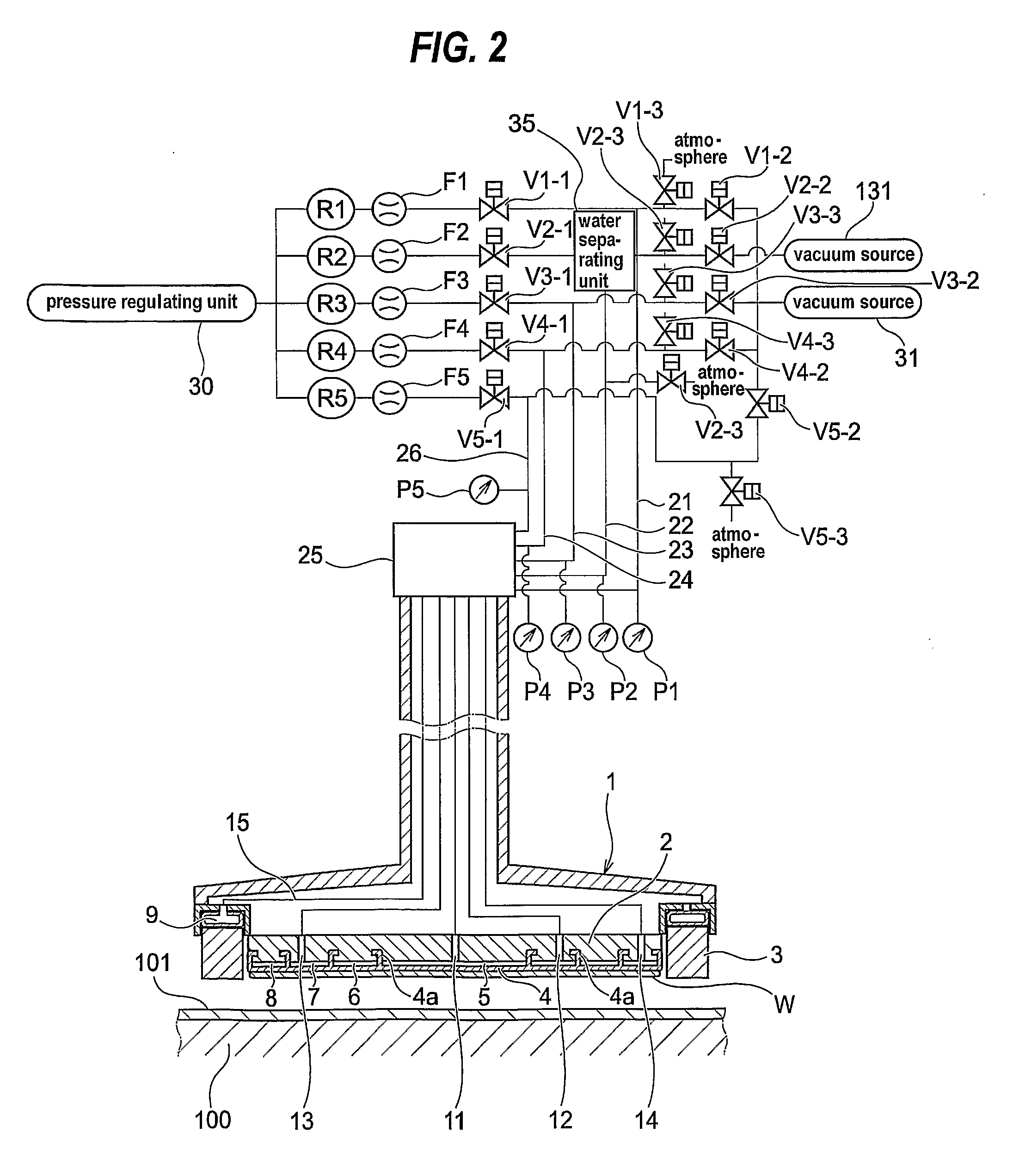
Further, if the pressure of the pressurizing chamber is not less than the membrane pressure at the time of polishing, the chucking plate presses the semiconductor
wafer locally, and a thin film on the semiconductor wafer is polished excessively in local regions thereof.
However, in use of this floating-type top ring, because the
pressure balance controls the position of the chucking plate, it is difficult to control the vertical position of the chucking plate precisely in the level of required for a recent fabrication process of highly miniaturized and multilayered device.
Further, the pressurizing chamber having a large volume requires sufficiently long time when application of the pressure to the semiconductor wafer is started or the semiconductor wafer is vacuum-chucked after polishing due to
prolongation of inflation or deflation process of the chamber, and there is a
lower limit for a volume of chamber for an appropriated balancing as described above.
This is thought to impede an improvement in productivity of the polishing apparatus.
Further, in the floating-type top ring, as wear of the
retainer ring progresses, the distance between the polishing surface and the lower surface of the chucking plate is shortened, and the amount of expansion and contraction of the membrane in the vertical direction varies locally, thus causing variation of the polishing profile.
However, the conventional polishing method thus conducted has the following problems unforeseen at first.
A gap between the semiconductor wafer and the polishing pad when application of the pressure to the semiconductor wafer is started may result in deformation of the semiconductor wafer.
Therefore, stress applied to the semiconductor wafer increases in such case, resulting in increase of breakage of fine interconnections formed on the semiconductor wafer or damage of the semiconductor wafer itself.
Therefore, stress applied to the semiconductor wafer increases and the semiconductor wafer is damaged in some cases in operation of membrane-type top ring.
However, a challenge to avoid such defect has not been successful so far.
Firstly, to form no gap is not successful: when pressure is applied to the semiconductor wafer or the semiconductor wafer is vacuum-chucked, if the top ring is lowered to the position where there is almost no gap between the semiconductor wafer and the polishing pad or the semiconductor wafer is brought into contact with the polishing pad locally, then a thin film on the semiconductor wafer is polished excessively or the semiconductor wafer itself is damaged at the worst.
Accordingly, stress tends to be applied to the semiconductor wafer locally in accordance with inflation of membrane, and fine interconnections formed on the semiconductor wafer are broken or the semiconductor wafer itself is damaged at the worst in use of these conventional top rings having
nozzle.

