

Aspect ratio adjustment of mask pattern using trimming to alter geometry of photoresist features
- Summary
- Abstract
- Description
- Claims
- Application Information
AI Technical Summary
Benefits of technology
Problems solved by technology
Method used
Image

Examples
example
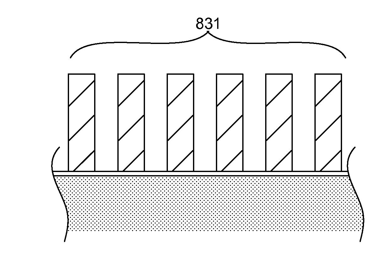
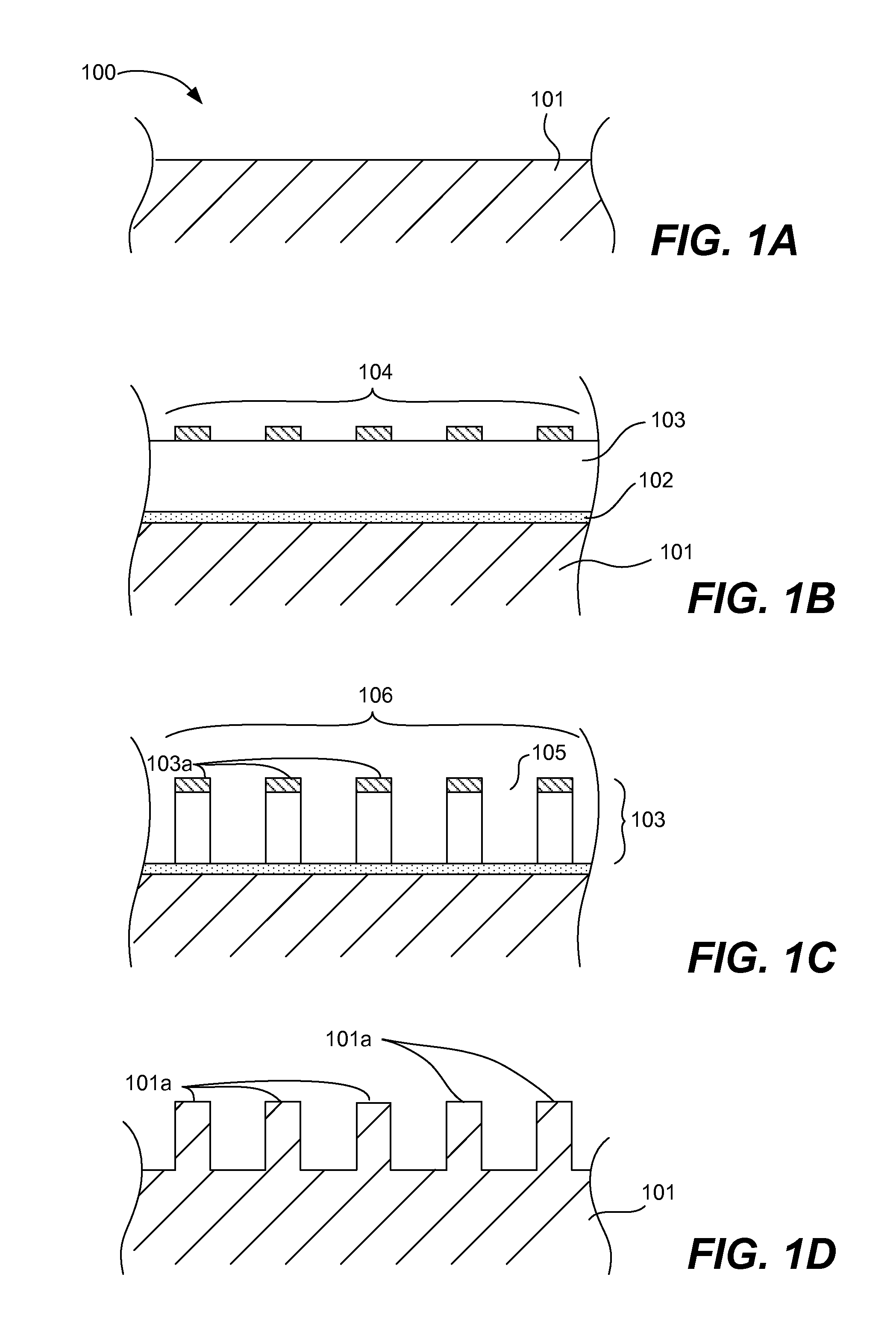
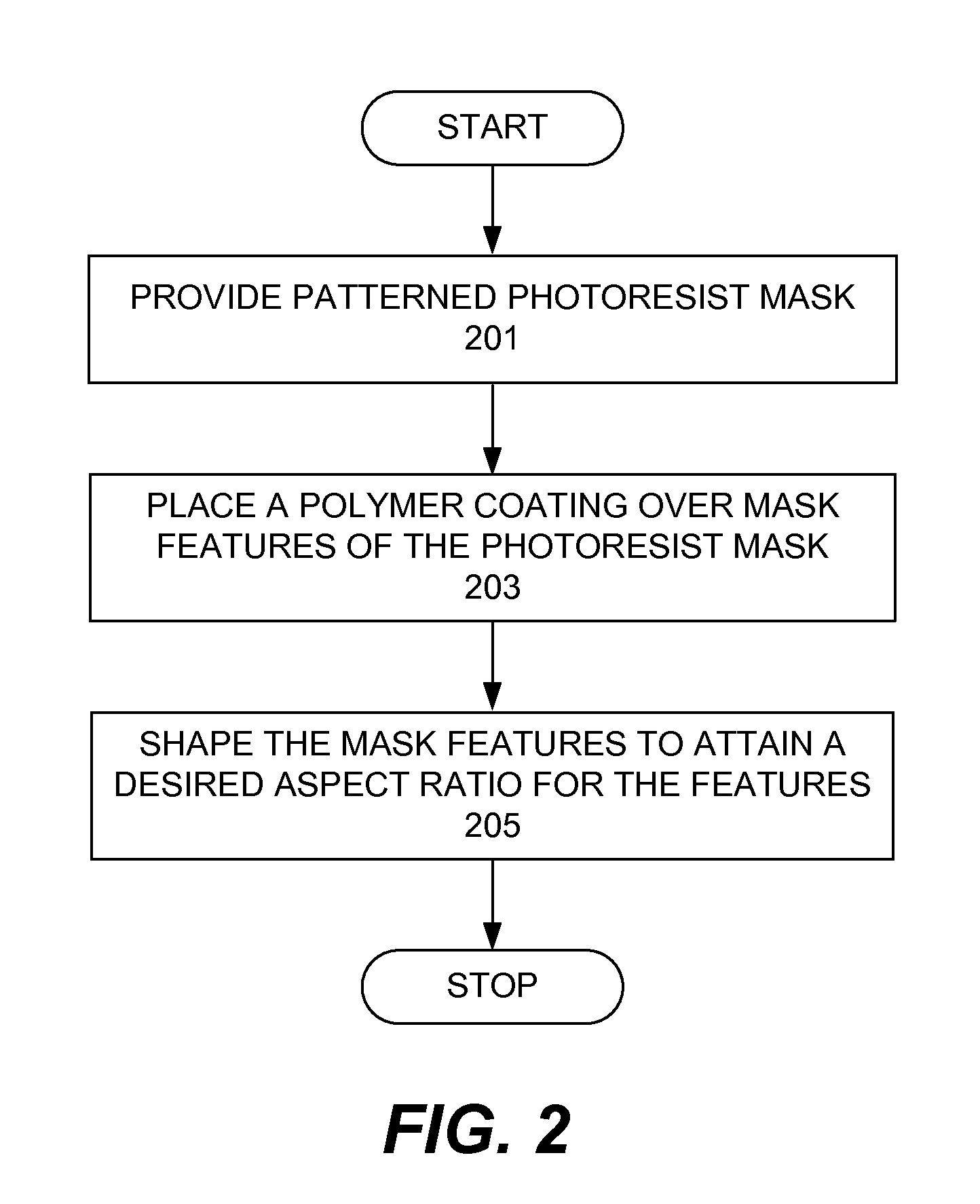
[0036]In an example of this process, a patterned photoresist layer is formed (Step 201). A substrate 300 having an underlayer 301 and a patterned photoresist mask 310 is placed in a processing chamber of an inductive coupled power (ICP) plasma processing device.
[0037]FIG. 5 is a schematic view of a plasma processing system 500 that may be used for placing a polymer layer over a photoresist mask and trimming the photoresist mask features. Plasma processing system 500 may include a plasma processing tool 501 which is an inductively coupled plasma processing tool and includes a plasma reactor processing chamber 504 therein. A transformer coupled power (TCP) controller 550 and a bias power controller 555, respectively, control a TCP power supply 551 and a bias power supply 556 influencing the plasma 524 created within plasma chamber 504.
[0038]The TCP power controller 550 sets a set point for TCP power supply 551 configured to supply a radio frequency signal at 13.56 MHz, tuned by a TCP ...
PUM
 Abstract
Description
Claims
Application Information