Bonded structure employing metal semiconductor alloy bonding

a technology of metal semiconductor and alloy bonding, which is applied in the direction of coatings, metallic pattern materials, solid-state devices, etc., can solve the problems of reliability problems in the bonded structure, limited bonding strength provided by conventional methods of substrate bonding, and short circuits of electrical shorts

Active Publication Date: 2011-07-14
IBM CORP
View PDF32 Cites 43 Cited by
  • Summary
  • Abstract
  • Description
  • Claims
  • Application Information

AI Technical Summary

Problems solved by technology

Diffusion of the conductive material from a TSV structure into the surrounding substrate region can cause electrical shorts and reliability problems in the bonded structure.
Because the diffusion of materials across a bonding interface is thermally driven and the

Method used


Image

  • Bonded structure employing metal semiconductor alloy bonding
  • Bonded structure employing metal semiconductor alloy bonding
  • Bonded structure employing metal semiconductor alloy bonding

Examples


first embodiment

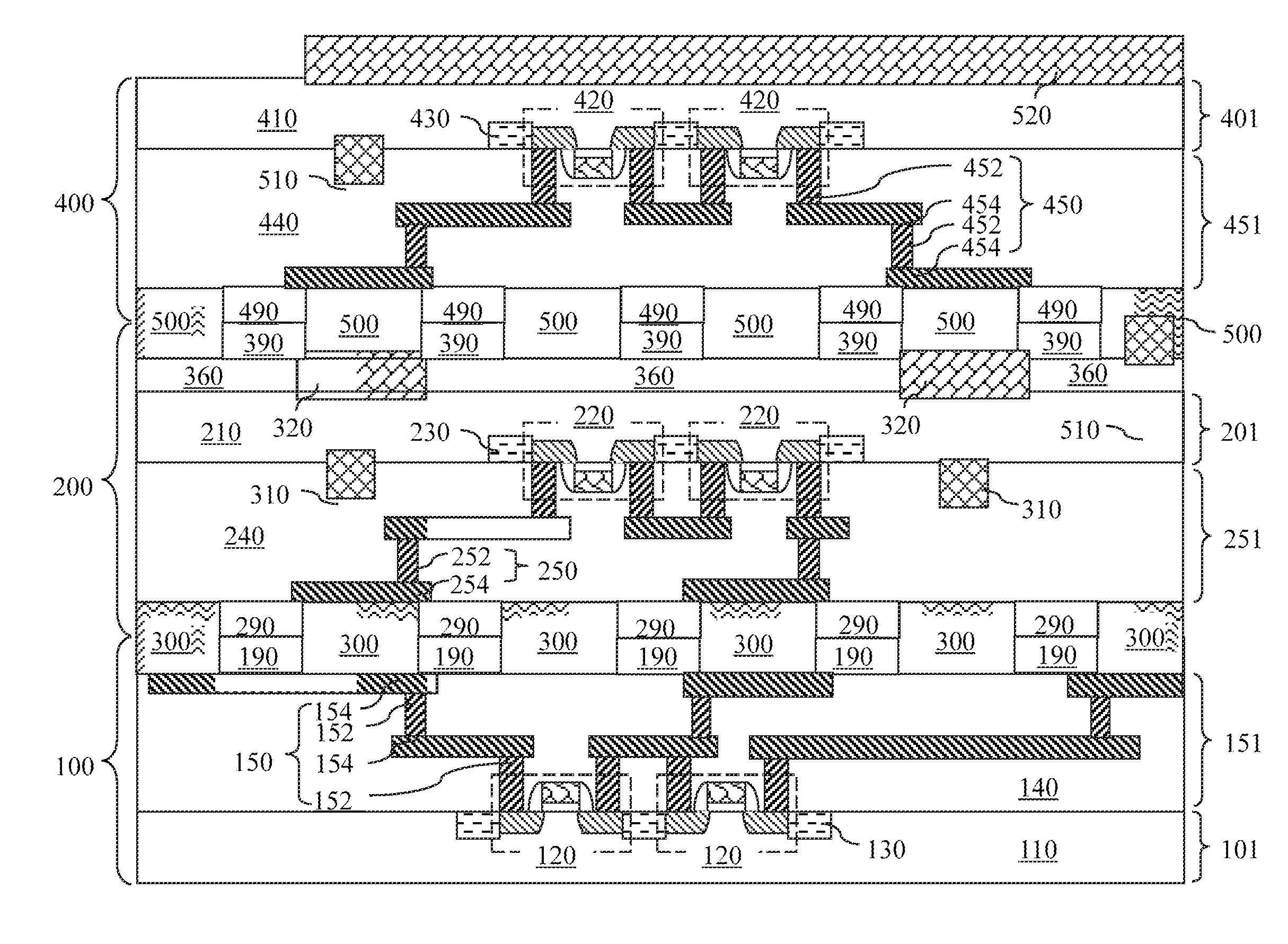
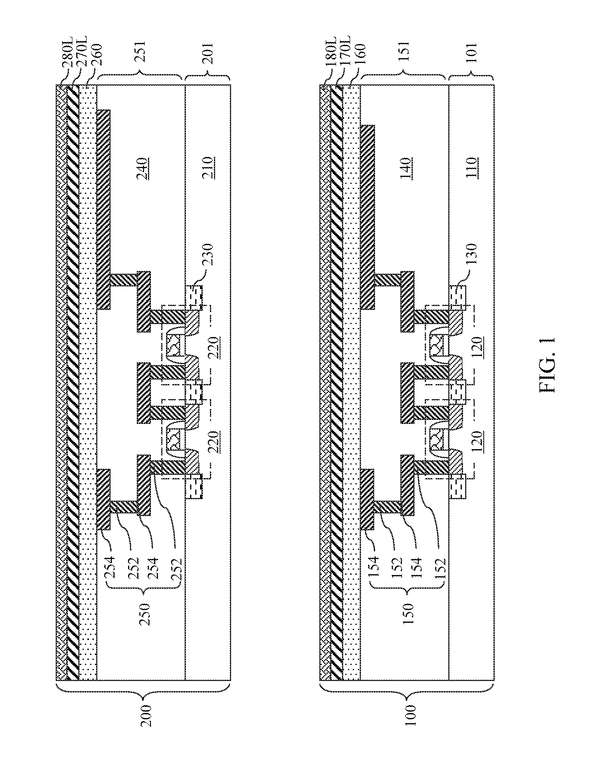
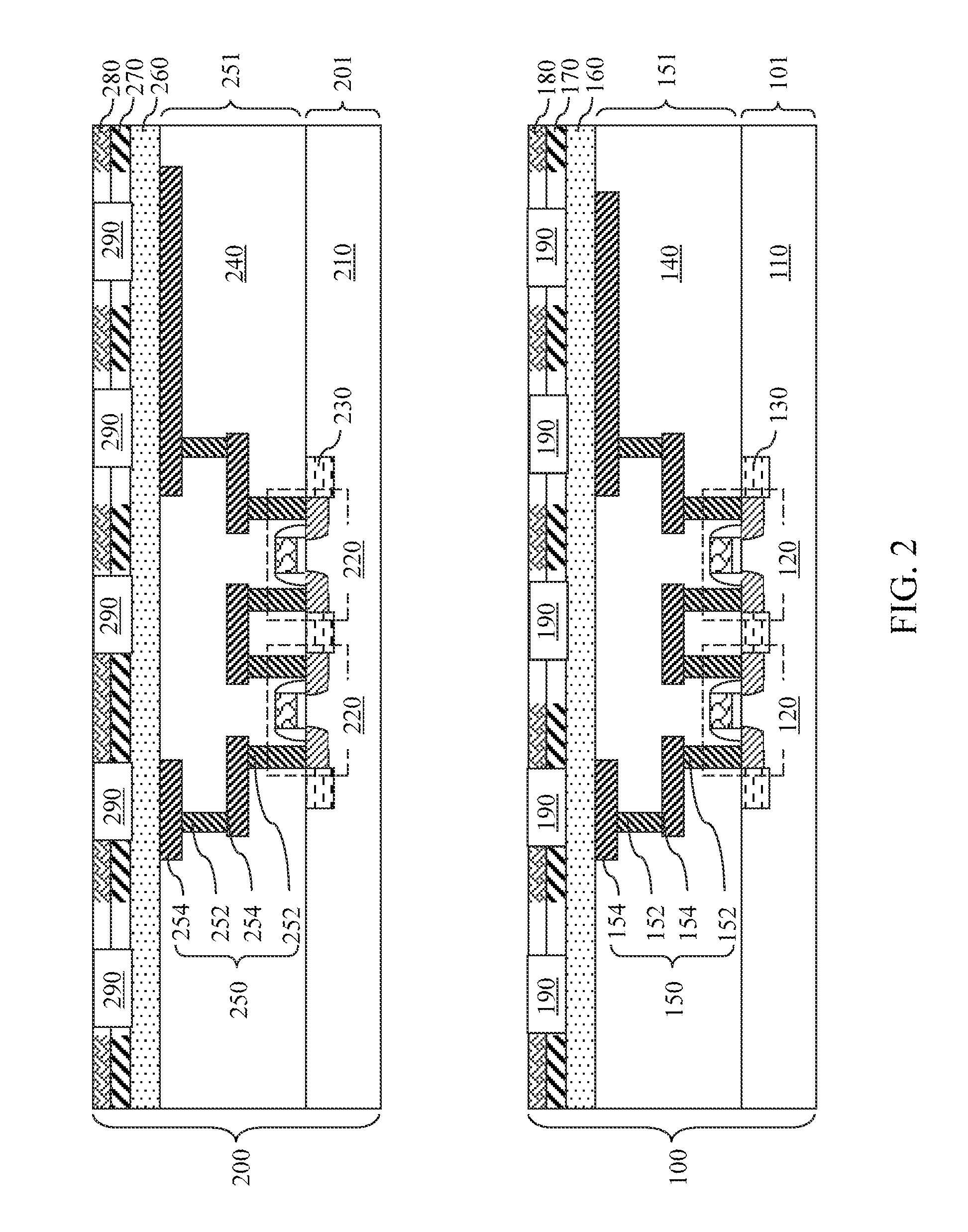
[0030]Referring to FIG. 1, a first exemplary structure according to the present invention includes a first substrate 100 and a second substrate 200 that are separated from each other. The first substrate 100 can include a first semiconductor substrate 101 and a first interconnect-level structure 151. The second substrate 200 can include a second semiconductor substrate 201 and a second interconnect-level structure 251.

[0031]The first semiconductor substrate 101 includes a first semiconductor layer 110. At least one first semiconductor device 120 can be present on the first semiconductor layer 110.

[0032]Likewise, the second semiconductor substrate 201 includes a second semiconductor layer 210. At least one second semiconductor device 220 can be present on the second semiconductor layer 210. Each of the at least one first semiconductor device 120 and the at least one second semiconductor device 220 can be, but is not limited to, a field effect transistor, a bipolar transistor, a diode...

second embodiment

[0057]Referring to FIG. 6, a second exemplary structure according to the present invention can be provided by modifying the process of forming the first exemplary structure of FIG. 1. Specifically, instead of forming a first metal layer 170L and a second metal layer 180L (See FIG. 1), a first dielectric material portions 190 is formed on the first substrate 100. The first dielectric material portions 190 can be formed, for example, by depositing a first dielectric material layer (not shown) on a surface of the first substrate 100 as a contiguous blanket layer, and by patterning the first dielectric material layer to form trenches therein. The first dielectric material portions 190 are formed on the first substrate 100, and the first dielectric material portions 190 are laterally spaced by the trenches.

[0058]Likewise, instead of forming a second metal layer 270L and a second metal layer 280L (See FIG. 1), a second dielectric material portions 290 is formed on the second substrate 200...

fourth embodiment

[0070]Referring to FIG. 11, a fourth exemplary structure according to the present invention includes a vertical stack of a first planar dielectric layer 160, a first metal layer 170L, and a first semiconductor layer 180L, which is formed on an exposed surface of a first semiconductor substrate 201, i.e., on an opposite side of a first interconnect-level structure 151. The first semiconductor substrate 101 is more proximal to the first semiconductor layer 180L than the first interconnect-level structure 151. Likewise, a vertical stack of a second planar dielectric layer 260, a second metal layer 270L, and a second semiconductor layer 280L is formed on an exposed surface of a second semiconductor substrate 202, i.e., on an opposite side of a second interconnect-level structure 251. The second semiconductor substrate 201 is more proximal to the second semiconductor layer 280L than the second interconnect-level structure 251.

[0071]Referring to FIG. 12, first metal-containing material po...


PUM


Abstract

Vertical stacks of a metal portion and a semiconductor portion formed on a first substrate are brought into physical contact with vertical stacks of a metal portion and a semiconductor portion formed on a second substrate. Alternately, vertical stacks of a metal portion and a semiconductor portion formed on a first substrate are brought into physical contact with metal portions formed on a second substrate. The assembly of the first and second substrates is subjected to an anneal at a temperature that induces formation of a metal semiconductor alloy derived from the semiconductor portions and the metal portions. The first substrate and the second substrate are bonded through metal semiconductor alloy portions that adhere to the first and second substrates.

Description

BACKGROUND[0001]This invention relates to a bonded structure that provides bonding between multiple substrates through formation of a metal semiconductor alloy and methods of manufacturing the same.[0002]Bonding of multiple substrates is required to enable three-dimensional integration of chips. Bonding of two substrates can be achieved by adhesion of two dielectric materials as in an oxide-to-oxide bonding that fuses silicon dioxide materials from two substrates after bonding, by adhesion between two metallic material as in a copper-to-copper bonding that employs direct contact between opposing copper pads and a subsequent grain growth across the original interface between the opposing copper pads, or by a method employing a combination of the two adhesion mechanisms.[0003]Through-substrate-via (TSV) structures, formed after multiple substrates are bonded and optionally thinned, provide electrical connection across the multiple substrates in a bonded structure. A TSV structure may ...

Claims


Application Information

Patent Timeline
IPC IPC(8): H05K1/09B05D5/12H05K1/02
CPCH01L21/2007H01L21/76841H01L27/0688H01L2224/80357H01L2224/80895H01L2224/80896H01L2224/80986
Inventor FAROOQ, MUKTA G.LI, ZHENGWENLUO, ZHIJIONGZHU, HUILONG
Owner IBM CORP
Why Eureka
Try Eureka