Silicon carbide substrate

Inactive Publication Date: 2011-07-21
SUMITOMO ELECTRIC IND LTD
View PDF1 Cites 0 Cited by
  • Summary
  • Abstract
  • Description
  • Claims
  • Application Information

AI Technical Summary

Benefits of technology

[0010]The present invention was made in view of the above-described problems, and an object of the presen

Problems solved by technology

A size of an SiC single-crystal substrate industrially remains as small as approximately 100 mm (4 inches) and hence it has not yet been able to efficiently manufacture a semiconductor device with the use of a large-sized single-crystal substrate.
In making use of characteristics of a plane other than a (0001) plane in particular in hexagonal SiC, the problem above is particularly serious, which will be described below.
It is thus difficult to secure a sufficient size of

Method used


Image

  • Silicon carbide substrate
  • Silicon carbide substrate
  • Silicon carbide substrate

Examples


first embodiment

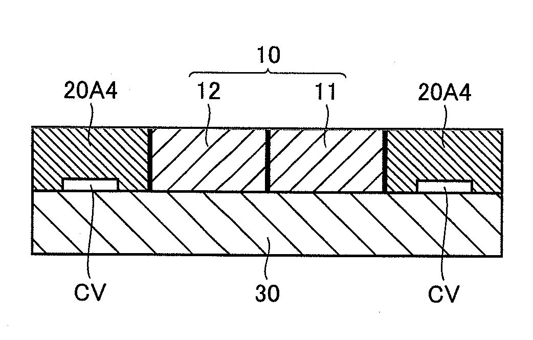
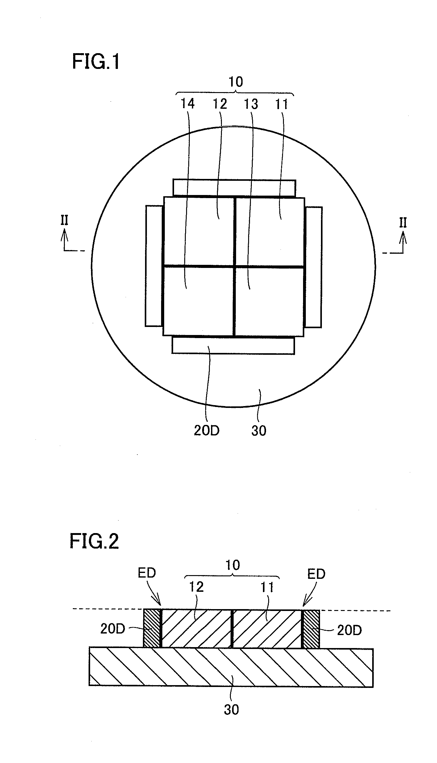
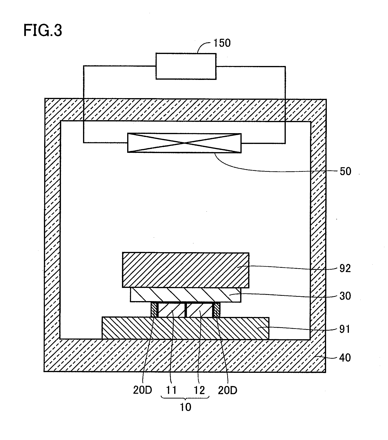
[0037]Referring to FIGS. 1 and 2, a silicon carbide substrate according to the present embodiment includes a base portion 30, silicon carbide layers 11 to 14 (collectively also referred to as group of layers 10), and a protection layer 20D.

[0038]Base portion 30 is made of silicon carbide and has a main surface (an upper surface in FIG. 2). Base portion 30 may be higher in dislocation density than each of silicon carbide layers 11 to 14, and thus base portion 30 having a large area can more readily be fabricated. In addition, under such a condition that dislocation density of base portion 30 may be high, base portion 30 can readily be higher in impurity concentration than each of silicon carbide layers 11 to 14, and thus conductivity of the silicon carbide substrate can be enhanced.

[0039]Each of silicon carbide layers 11 to 14 is provided on the main surface of base portion 30 in a manner exposing a region of the main surface of base portion 30, along an outer edge of the main surfac...

second embodiment

[0056]Referring mainly to FIG. 4, a silicon carbide substrate according to the present embodiment has a plurality of protection layers 20S instead of protection layer 20D (FIG. 1) in the first embodiment. Protection layers 20S surround group of layers 10 constituted of silicon carbide layers 11 to 14 on the main surface of base portion 30. Since the construction other than the above is substantially the same as in the first embodiment described above, the same or corresponding elements have the same reference characters allotted and description thereof will not be repeated. According to the present embodiment, during polishing of the surface of the silicon carbide substrate, excessive polishing can be suppressed in the entire portion of the surface of silicon carbide layers 11 to 14, that is close to the outer edge of base portion 30.

third embodiment

[0057]Referring mainly to FIG. 5, a silicon carbide substrate according to the present embodiment has a protection layer 20F instead of the plurality of protection layers 20S (FIG. 4) in the second embodiment. Protection layer 20F has such a shape that the plurality of protection layers 20S are integrated. Therefore, protection layer 20F has a continuous loop shape. Since the construction other than the above is substantially the same as that in the second embodiment described above, the same or corresponding elements have the same reference characters allotted and description thereof will not be repeated. According to the present embodiment, excessive polishing can be suppressed by a single protection layer 20F in the entire portion of the respective surfaces of silicon carbide layers 11 to 14, that is close to the outer edge of base portion 30.


PUM


Abstract

A base portion is made of silicon carbide and has a main surface. At least one silicon carbide layer is provided on the main surface of the base portion in a manner exposing a region of the main surface along an outer edge of the main surface. At least one protection layer is provided on this region of the main surface of the base portion along the outer edge of the main surface. Thus, a silicon carbide substrate can be polished with high in-plane uniformity.

Description

BACKGROUND OF THE INVENTION[0001]1. Field of the Invention[0002]The present invention relates to a silicon carbide substrate.[0003]2. Description of the Background Art[0004]An SiC (silicon carbide) substrate has recently increasingly been adopted as a semiconductor substrate used for manufacturing a semiconductor device. SiC has a bandgap wider than Si (silicon) that has more commonly been used. Therefore, a semiconductor device including an SiC substrate is advantageous in a high reverse breakdown voltage, a low ON resistance and less lowering in characteristics in an environment at a high temperature.[0005]In order to efficiently manufacture a semiconductor device, a substrate is required to have a size not smaller than a certain size. According to U.S. Pat. No. 7,314,520, an SiC substrate not smaller than 76 mm (3 inches) can be manufactured.[0006]A size of an SiC single-crystal substrate industrially remains as small as approximately 100 mm (4 inches) and hence it has not yet be...

Claims


Application Information

Patent Timeline
IPC IPC(8): H01L29/16
CPCH01L21/02002H01L21/02378H01L29/1608H01L21/02667H01L21/30625H01L21/02529
Inventor NISHIGUCHI, TAROSASAKI, MAKOTOHARADA, SHINOKITA, KYOKOINOUE, HIROKIFUJIWARA, SHINSUKENAMIKAWA, YASUO
Owner SUMITOMO ELECTRIC IND LTD
Why Eureka
Try Eureka