SiC EPITAXIAL WAFER AND METHOD FOR MANUFACTURING SIC EPITAXIAL WAFER

Pending Publication Date: 2022-05-12
SHOWA DENKO KK
View PDF0 Cites 0 Cited by
  • Summary
  • Abstract
  • Description
  • Claims
  • Application Information

AI Technical Summary

Benefits of technology

The present invention provides a method for manufacturing aSiC epitaxial wafer with high uniformity in n-type doping concentration. This results in a more consistent and reliable material for use in various applications.

Problems solved by technology

For that reason, in large-current power devices whose market is expected to expand in the future, simply converting the basal plane dislocations into the TEDs cannot sufficiently inhibit formation of the SFs, and there is always a concern of deterioration in reliability of the device.
The elongation and expansion of the BPDs are a cause of forward deterioration of a device.
However, it does not mention in-plane uniformity in doping concentration of a high concentration layer.

Method used


Image

  • SiC EPITAXIAL WAFER AND METHOD FOR MANUFACTURING SIC EPITAXIAL WAFER
  • SiC EPITAXIAL WAFER AND METHOD FOR MANUFACTURING SIC EPITAXIAL WAFER
  • SiC EPITAXIAL WAFER AND METHOD FOR MANUFACTURING SIC EPITAXIAL WAFER

Examples


Embodiment Construction

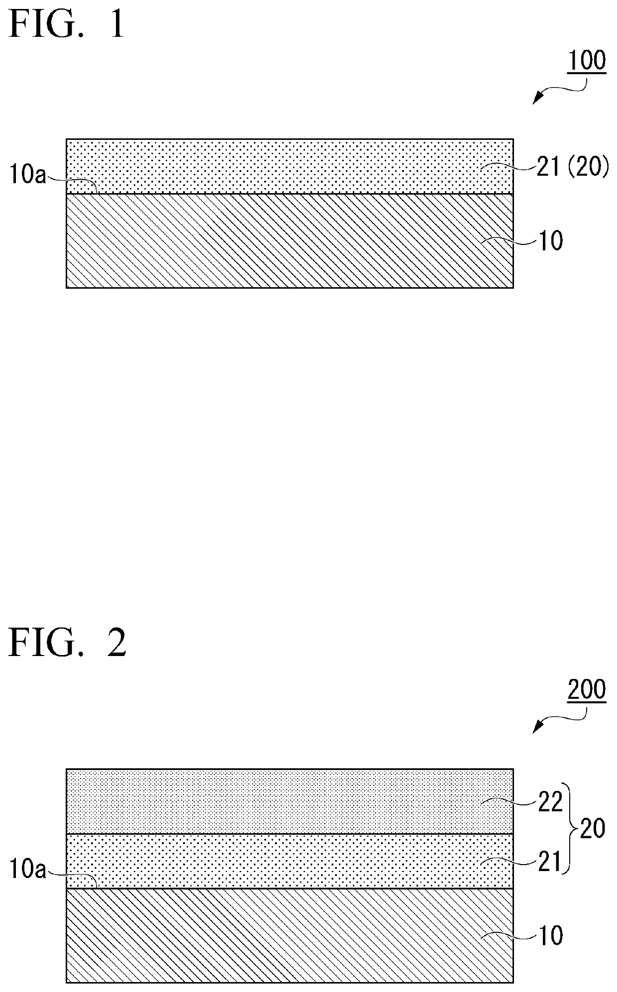
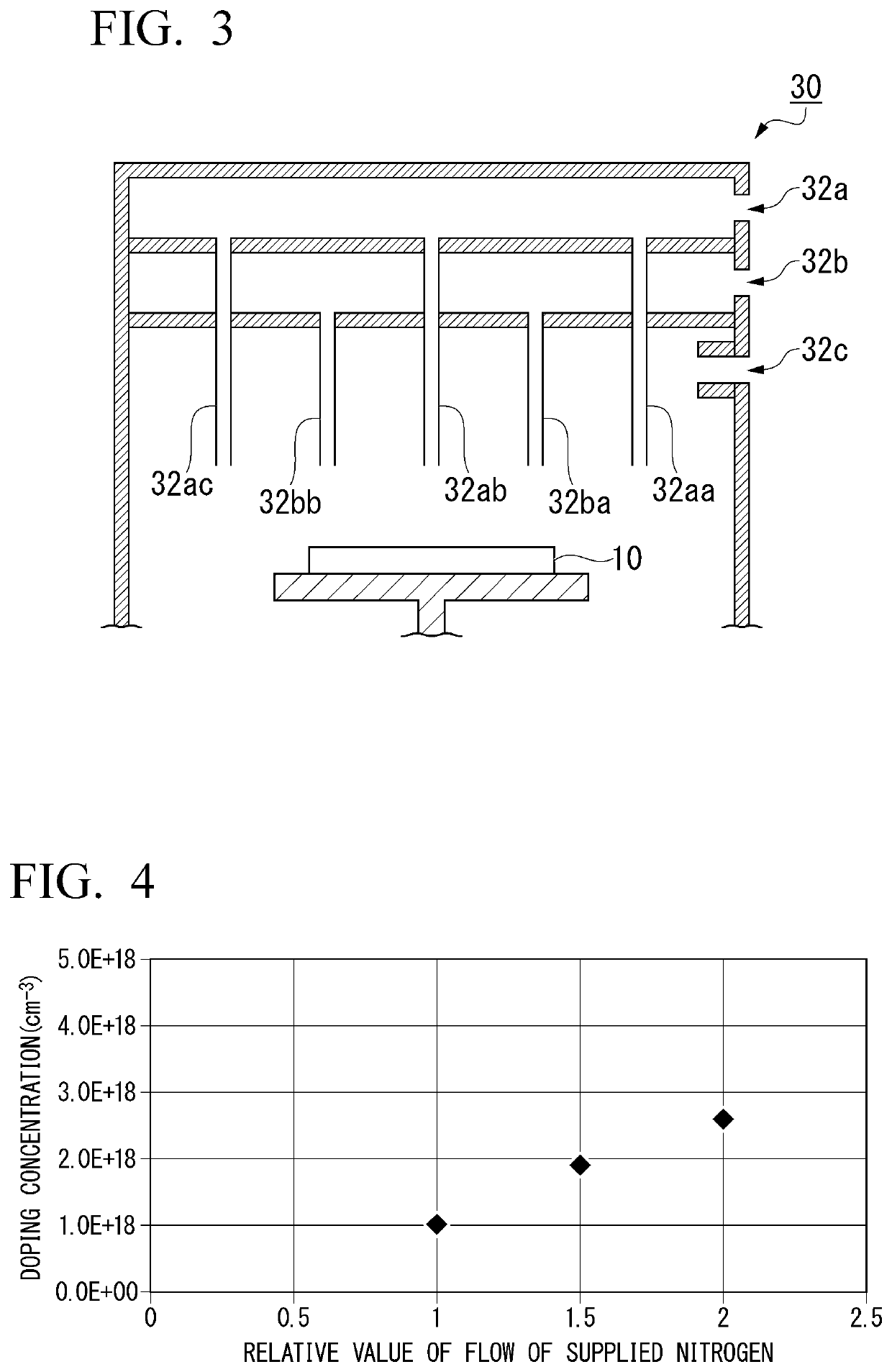
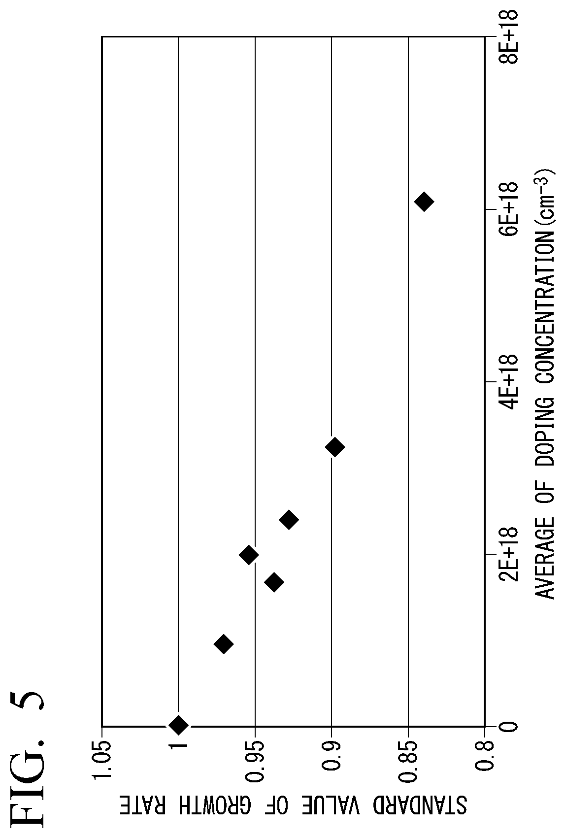
[0043]Hereinafter, examples of preferred embodiments of the present invention will be described with reference to the drawings. In addition, in each of the following embodiments, the same or equivalent parts may be designated by the same reference numerals in the drawings. Also, in the drawings used in the following description, featured portions may be enlarged for convenience in order to make the features easy to understand, and dimensional ratios and the like of each component are not always the same as actual ones. Further, materials, dimensions, and the like exemplified in the following description are examples, and the present invention is not limited thereto but can be carried out with appropriate changes as long as the effects of the present invention are achieved. A configuration shown in one embodiment can also be applied to other embodiments. For example, the present invention is not limited to the following examples, and additions, omissions, substitutions, and changes c...


PUM

PropertyMeasurementUnit
Fractionaaaaaaaaaa
Fractionaaaaaaaaaa
Fractionaaaaaaaaaa

Abstract

A SiC epitaxial wafer of the present invention includes a SiC single crystal substrate, and a high concentration layer that is provided on the SiC single crystal substrate and has an average value of an n-type doping concentration of 1×10¹⁸ / cm3 or more and 1×10¹⁹ / cm3 or less, and in-plane uniformity of the doping concentration of 30% or less.

Description

BACKGROUND OF THE INVENTIONField of the Invention[0001]The present invention relates to a SiC epitaxial wafer and a method for manufacturing the same.[0002]Priority is claimed on Japanese Patent Application No. 2020-188693, filed Nov. 12, 2020, the content of which is incorporated herein by reference.Description of Related Art[0003]Silicon carbide (SiC) has a dielectric breakdown electric field that is one order of magnitude larger, a bandgap that is three times larger, and a thermal conductivity that is about three times higher than silicon (Si). For this reason, silicon carbide (SiC) is expected to be applied to power devices, high frequency devices, high temperature operation devices, and the like.[0004]In order to promote the practical application of SiC devices, it is required to establish high-quality and low-cost SiC epitaxial wafers and epitaxial growth technology.[0005]SiC devices are formed by using a SiC epitaxial wafer that includes a SiC substrate and an epitaxial layer...

Claims


Application Information

Patent Timeline
IPC IPC(8): H01L29/36H01L29/16H01L21/02
CPCH01L29/365H01L29/1608H01L21/0262H01L21/02529H01L21/02584H01L21/02378H01L21/02598C30B25/14C30B25/16C30B29/36C30B25/165C23C16/52C23C16/325C23C16/45565C23C16/45574H01L21/02576H01L21/02579H01L21/02502H01L21/02447H01L21/02433
Inventor ISHIBASHI, NAOTOFUKADA, KEISUKE
Owner SHOWA DENKO KK
Why Eureka
Try Eureka