Photoelectric conversion device and solar cell having the same

a conversion device and solar cell technology, applied in the direction of solid-state devices, semiconductor devices, electrical devices, etc., can solve the problems of degradation of photoelectric conversion efficiency, difficult formation of buffer layers on ci(g)s, uneven surface, etc., to achieve high photoelectric conversion efficiency, increase the uniformity of buffer layers, and improve the effect of compactness

Inactive Publication Date: 2013-10-17
FUJIFILM CORP
View PDF1 Cites 1 Cited by
  • Summary
  • Abstract
  • Description
  • Claims
  • Application Information

AI Technical Summary

Benefits of technology

[0035]In the photoelectric conversion device of the present invention, a carbonyl ion is provided on a surface of the buffer layer on the side of the transparent conductive layer, and the buffer layer is a thin film layer with an average film thickness of 10 nm to 70 nm and includes a ternary compound of a cadmium-free metal, oxygen, and sulfur. According to such arrangement, the compactness of the buffer layer is increased by the presence of the carbonyl ion and the buffer layer may uniformly cover the under layer. Thus, according to the present invention, a photoelectric conversion device having high photoelectric conversion efficiency and high in-plane uniformity thereof may be provided.
[0036]Further, such buffer layer may be formed under moderate alkaline conditions, so that a base material which includes a metal easily soluble in an alkaline solvent, such as aluminum, may be used as the substrate. Therefore, an embodiment having a substrate that includes a thin and highly flexible aluminum metal may provide a flexible photoelectric conversion device having high in-plane uniformity of photoelectric conversion efficiency.

Problems solved by technology

As described above, it is difficult to form a buffer layer on a CI(G)S photoelectric conversion semiconductor layer having relatively large surface unevenness as a uniform film without any gap.
A defect in the buffer layer, such as a gap or crack, may cause problems, such as degradation in the photoelectric conversion efficiency due to loss of buffering effects in the defective portion, a variation in the photoelectric conversion efficiency from cell to cell due to degraded in-plane homogeneity of photoelectric conversion efficiency, and the like.
In the aforementioned documents, the photoelectric conversion efficiency and uniformity thereof are not evaluated or otherwise favorable photoelectric conversion characteristics are not obtained.
Further, in forming Zn buffer layers by CBD process, it is one of the problems to improve production costs by increasing the reaction speed.
As the reaction solution used in Patent Document 8, however, is highly alkaline, substrates which include metals easily soluble in an alkaline solvent, such as metals, including aluminum, capable of forming a complex ion with a hydroxide ion, cannot be used.

Method used


Image

  • Photoelectric conversion device and solar cell having the same
  • Photoelectric conversion device and solar cell having the same
  • Photoelectric conversion device and solar cell having the same

Examples


examples

[0107]Examples and Comparative Examples of the present invention will now be described. As Examples 1 to 7 and Comparative Examples 1 to 6, buffer layers were formed using different combinations of substrate, reaction solution used for forming buffer layers by CBD process, and CBD reaction condition, and the buffer layers so formed were evaluated. Hereinafter, substrates, preparation method of CBD reaction solutions, and reaction conditions used for Examples and Comparative Examples will be described first followed by the evaluation methods and results.

[0108]As for substrates, two types of substrates were provided.

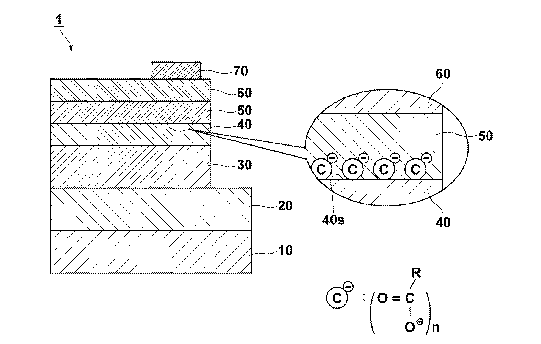
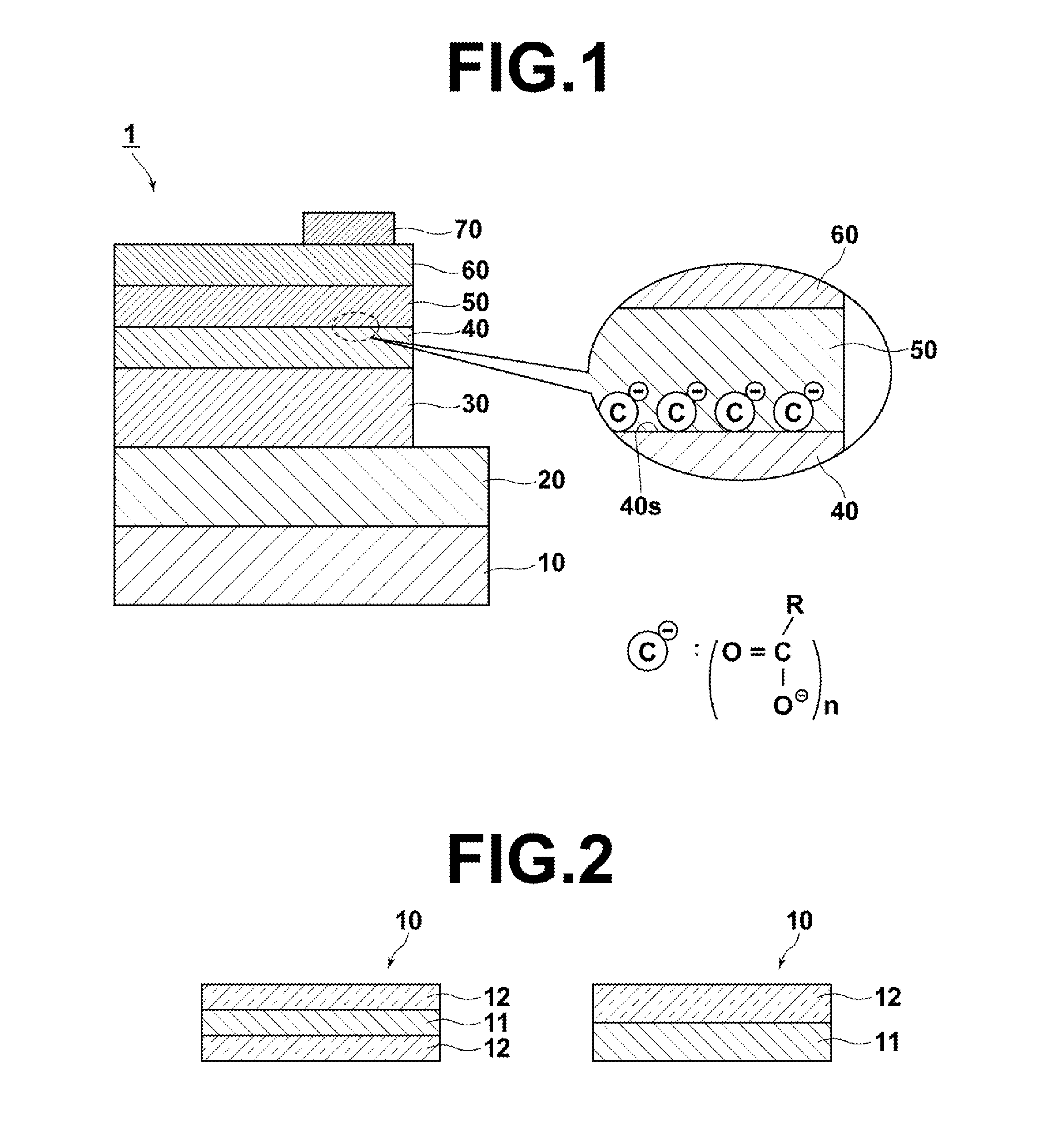
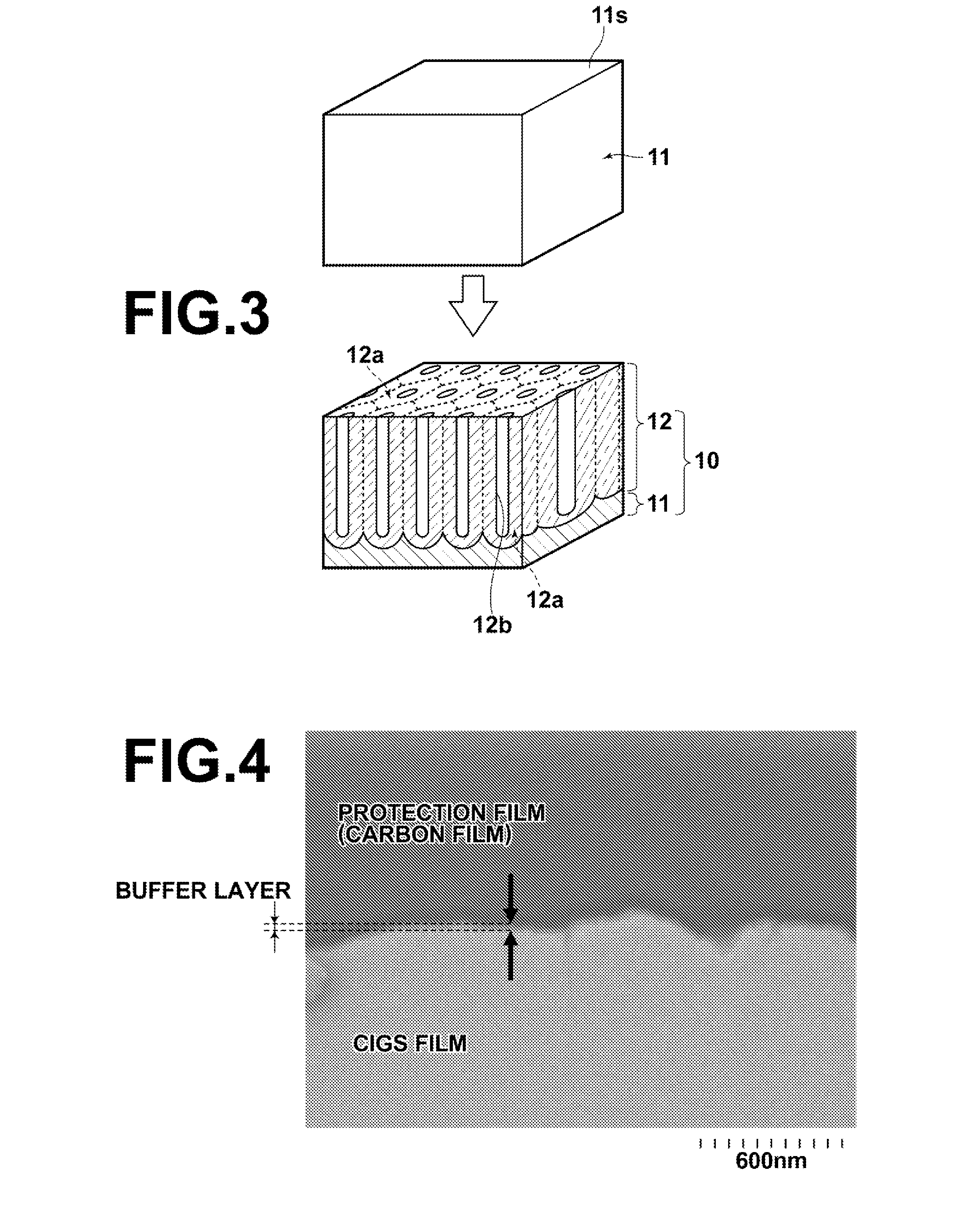
[0109](1) Cu(In0.7Ga0.3)Se2 / Mo / SLG / AAO / Al / SUS substrate: substrate that uses an anodized substrate (30 mm×30 mm) made of a composite base of a 100 μm thick stainless steel (SUS) and a 30 μm thick Al with an anodized aluminum film (AAO) formed on the surface of the Al, and a soda lime glass (SLG) layer, a Mo electrode layer, and a CIGS layer are further formed on the surfac...


PUM


Abstract

The photoelectric conversion device of the present invention is a photoelectric conversion device which includes a substrate on which the following are layered in the order listed below: a lower electrode layer; a photoelectric conversion semiconductor layer which includes, as a major component, at least one kind of compound semiconductor having a chalcopyrite structure formed of a group Ib element, a group IIIb element, and a group VIb element; a buffer layer; and a transparent conductive layer, in which a carbonyl ion is provided on a surface of the buffer layer on the side of the transparent conductive layer and the buffer layer is a thin film layer having an average film thickness of 10 nm to 70 nm and includes a ternary compound of a cadmium-free metal, oxygen, and sulfur.

Description

TECHNICAL FIELD[0001]The present invention relates to a photoelectric conversion device and a solar cell having the same.BACKGROUND ART[0002]Photoelectric conversion devices having a photoelectric conversion layer and electrodes in electrical communication with the layer are used in various applications including solar cells.[0003]Most of the conventional solar cells are Si-based cells that use bulk monocrystalline Si, polycrystalline Si, or thin film amorphous Si. Recently, however, research and development of compound semiconductor-based solar cells that do not depend on Si has been carried out. Two types of compound semiconductor-based solar cells are known, one of which is a bulk system, such as GaAs system and the like, and the other of which is a thin film system, such as CIS system formed of a group Ib element, a group IIIb element, and a group VIb element, CIGS, or the like. CI(G)S is a compound semiconductor represented by a general chemical formula, Cu1-zIn1-xGaxSe2-ySy(wh...

Claims


Application Information

Patent Timeline
Patent Type & Authority Applications(United States)
IPC IPC(8): H01L31/0328
CPCH01L31/0328H01L31/03923H01L31/0749Y02E10/541H01L31/04
Inventor KAWANO, TETSUOKAGA, HIROSHI
Owner FUJIFILM CORP
Why Eureka
Try Eureka