Infrared Sensor

a technology of infrared sensor and infrared sensor, which is applied in the field of infrared sensor, can solve the problems of infrared sensor structural stability and low sensitivity, increased power consumption, and infrared detection element is likely to suffer from warp, so as to prevent improve the fabrication yield. , the effect of preventing the breakage of infrared sensor

Inactive Publication Date: 2011-07-21
PANASONIC CORP
View PDF10 Cites 20 Cited by
  • Summary
  • Abstract
  • Description
  • Claims
  • Application Information

AI Technical Summary

Benefits of technology

[0036]According to this aspect, it is possible to prevent breakage of the infrared sensor which would otherwise occur due to a stress caused by an external temperature variation or impact at the time of using the infrared sensor. It is enabled to prevent breakage of the infrared sensor at the time of manufacturing the same. The fabrication yield can be improved.

Problems solved by technology

When the dielectric layer is thinned, the dielectric layer being the infrared absorption member is likely to suffer from a warp, and the infrared sensor may have poor structural stability and low sensitivity.
This causes increased power consumption.
Moreover, since the bolometer type infrared detection element heats itself, the infrared detection element is likely to suffer from a warp caused by thermal stress resulting from the self-heating.
However, to provide the temperature compensation polysilicon layer enlarges the infrared sensor, and increases a production cost.
Thus, the thermopile does not produce self-heating.
In this situation, a thin film structure comprising the infrared sensor and the thermopile formed thereon is likely to suffer from a warp, and the infrared sensor may have poor structural stability and low sensitivity.

Method used


Image

  • Infrared Sensor
  • Infrared Sensor
  • Infrared Sensor

Examples


first embodiment

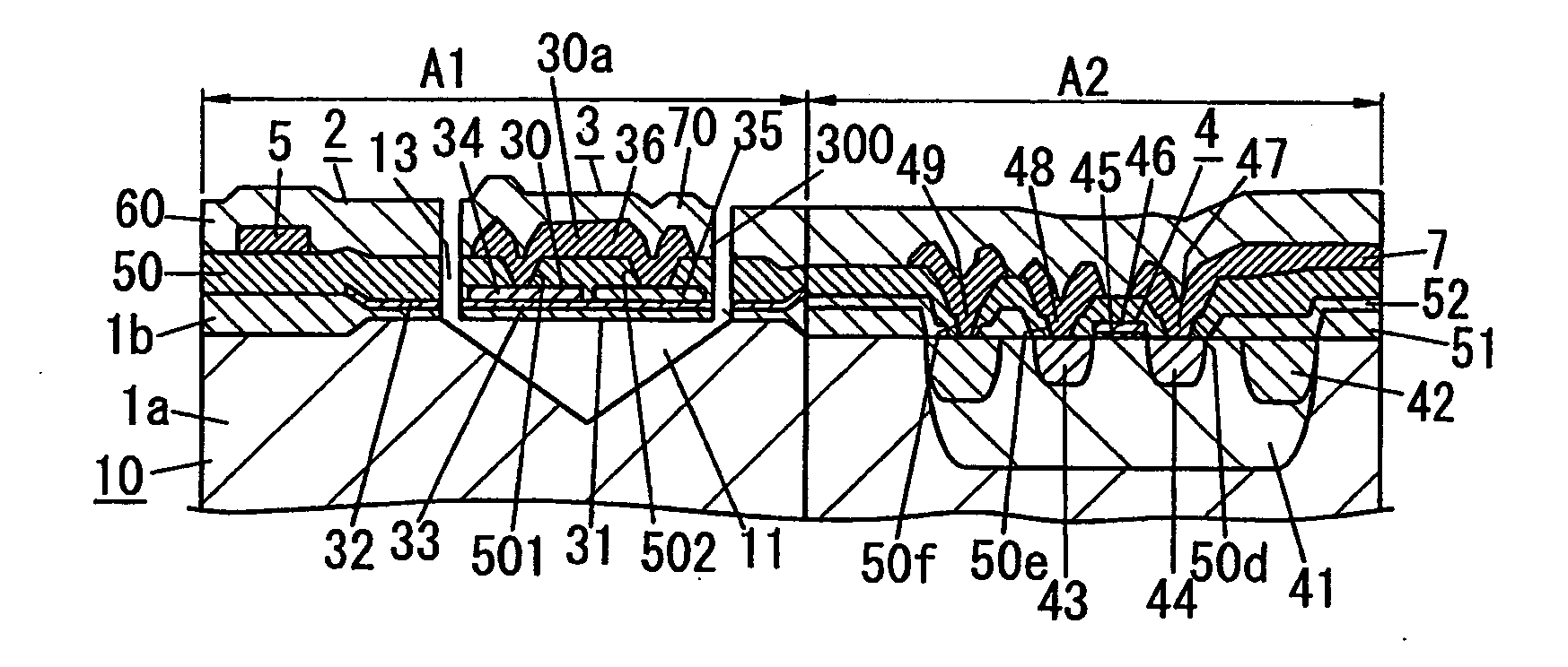
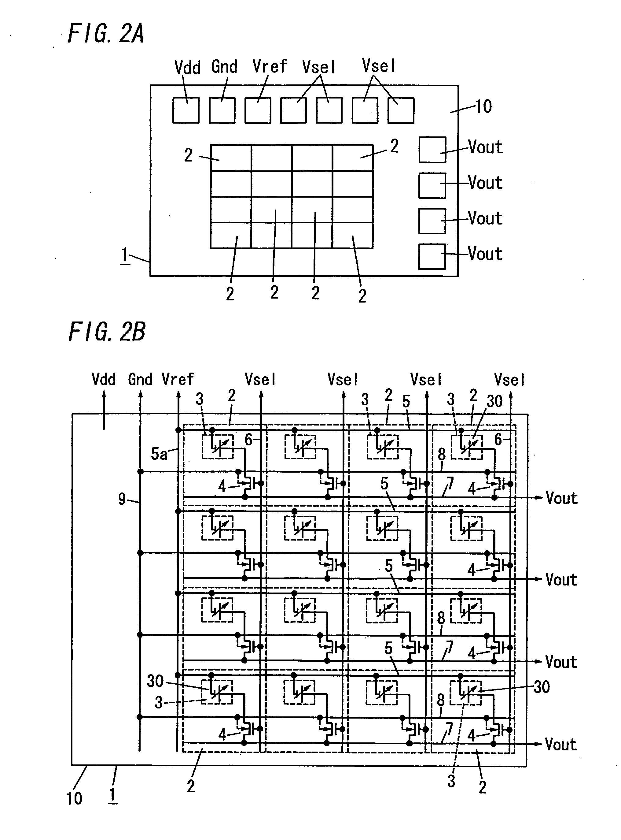
[0093]The infrared sensor 1 of the present embodiment is an infrared image sensor (infrared array sensor). As shown in FIGS. 1 and 2, the infrared sensor 1 includes a base (base substrate) 10 used as a basement, and a plurality of cells (pixels) 2 arranged on a first surface (upper surface, in FIG. 1B) of the base 10 in an array (two dimensional array, in the illustrated instance) manner. The cell 2 includes a thermal type infrared detection element 3 including an infrared absorption member 33 and a temperature detection member 30, and a MOS transistor 4 defined as a switching element for pixel selection.

[0094]In the present embodiment, m by n (4 by 4, in the illustrated instance) pixels 2 are formed on the first surface of the single base 10. The number, arrangement, or both of the pixels 2 is not limited to the present embodiment. Besides, in FIG. 2B, an equivalent circuit of the temperature detection member 30 is illustrated as a power source.

[0095]The infrared sensor 1 includes ...

second embodiment

[0149]The infrared sensor 1A of the present embodiment is different from the infrared sensor 1 of the first embodiment in the pixel 2A and the temperature detection member 30A. Configurations common to the infrared sensor 1A and the infrared sensor 1 are designated by the same reference numerals, and no explanations thereof are made.

[0150]Each of the pixels 2A is provided with no MOS transistor 4.

[0151]The temperature detection member 30A includes the four thermocouples 30a each of which includes an n-type polysilicon layer 34, a p-type polysilicon layer 35, and a connection layer 36. The second end of the p-type polysilicon layer 35 of the thermocouple 30a is connected to the second end of the n-type polysilicon layer 34 of the thermocouple 30a next thereto by use of a connection layer 37 made of a metal material (e.g., Al—Si). As described in the above, the four thermocouples 30a are connected in series with each other to constitute a thermopile.

[0152]The aforementioned thermopile...

third embodiment

[0160]The following explains the infrared sensor 1B of the present embodiment with reference to FIGS. 13 to 37.

[0161]The infrared sensor 1B of the present embodiment is mainly different from the infrared sensor 1 of the first embodiment in the thin film structure 300B. Besides, components common to the infrared sensor 1B and the infrared sensor 1 are designated by the same reference numerals, and no explanations thereof are made.

[0162]In the infrared sensor 1B, as shown in FIGS. 15 and 25, the 8 by 8 pixels 2 are formed over the first surface of the single base 10. The number and arrangement of the pixels 2 are not limited.

[0163]Besides, in FIG. 15, the pixel selections Vsel, the reference bias pad Vref, the ground pad Gnd, the output pads Vout, and the like are illustrated, with no distinction, as pads 81.

[0164]FIG. 26 shows the infrared sensor module including the infrared sensor 1B (infrared array sensor module). This infrared sensor module includes the infrared sensor 1B, the si...


PUM


Abstract

The infrared sensor (1) includes a base (10), and an infrared detection element (3) formed over a surface of the base (10). The infrared detection element (3) includes an infrared absorption member (33) in the form of a thin film configured to absorb infrared, a temperature detection member (30) configured to measure a temperature difference between the infrared absorption member (33) and the base (10), and a safeguard film (39). The infrared element (3) is spaced from the surface of the base (10) for thermal insulation. The temperature detection member (30) includes a p-type polysilicon layer (35) formed over the infrared absorption member (33) and the base (10), an n-type polysilicon layer (34) formed over the infrared absorption member (33) and the base (10) without contact with the p-type polysilicon layer (35), and a connection layer (36) configured to electrically connect the p-type polysilicon layer (35) to the n-type polysilicon layer (34). The safeguard film (39) is a polysilicon layer formed on an infrared incident surface defined as an opposite surface of the infrared absorption member (33) from the base (10) to cover the infrared incident surface.

Description

TECHNICAL FIELD [0001]The present invention relates to an infrared sensor.BACKGROUND ART[0002]In the past, there has been proposed an infrared sensor which detects infrared (e.g., infrared having a wavelength of 8 to 12 μm which emitted from a human body). A document 1 (Japanese patent publication No. 2576259) and a document 2 (Japanese patent publication No. 3287173) disclose infrared sensors manufactured by use of micromachining techniques. This kind of infrared sensor includes a thin film-shaped infrared absorption member and a temperature detection member. The infrared absorption member absorbs infrared and converts the absorbed infrared into heat. The temperature detection member measures a change in temperature of the infrared absorption member.[0003]The infrared sensor disclosed in the above document 1 includes a silicon substrate, and a silicon nitride film formed on the silicon substrate. The silicon substrate is provided with a cavity for thermal insulation. The silicon ni...

Claims


Application Information

Patent Timeline
Patent Type & Authority Applications(United States)
IPC IPC(8): H01L29/66H01L31/028
CPCG01J5/02G01J5/0225H01L2224/73265H01L2224/49175H01L2224/48137G01J5/06G01J5/08G01J5/0846G01J5/12G01J5/20H01L27/14649H01L27/14669H01L27/14692H01L2924/13091H01L2224/48091H01L2924/00014H01L2924/00H01L2224/05554H01L2924/16151H01L2924/16195G01J1/02H01L27/14H10N10/17
Inventor TSUJI, KOJIHAGIHARA, YOSUKEUSHIYAMA, NAOKI
Owner PANASONIC CORP
Why Eureka
Try Eureka