Nanostructured photodiode

Inactive Publication Date: 2011-07-28
QUNANO
View PDF2 Cites 62 Cited by
  • Summary
  • Abstract
  • Description
  • Claims
  • Application Information

AI Technical Summary

Benefits of technology

[0015]The performance and reliability of photodiodes according to the invention can be further improved by utilizing at least a portion of the nanowires as a current limiting structure based on space charge build-up in the nanowire portion. This space charge effect yields a sur

Problems solved by technology

The prior art large area photodetectors have drawbacks with regards to high dark curr

Method used


Image

  • Nanostructured photodiode
  • Nanostructured photodiode
  • Nanostructured photodiode

Examples


Embodiment Construction

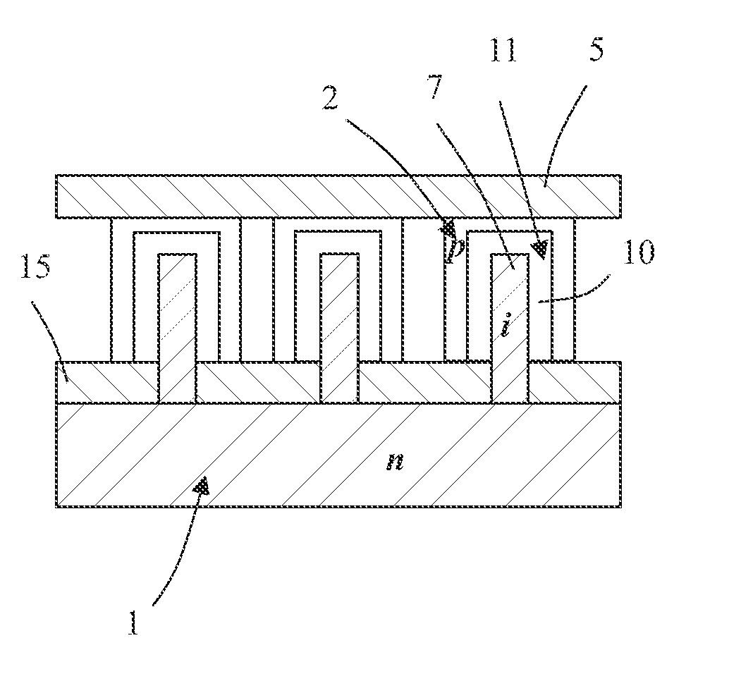
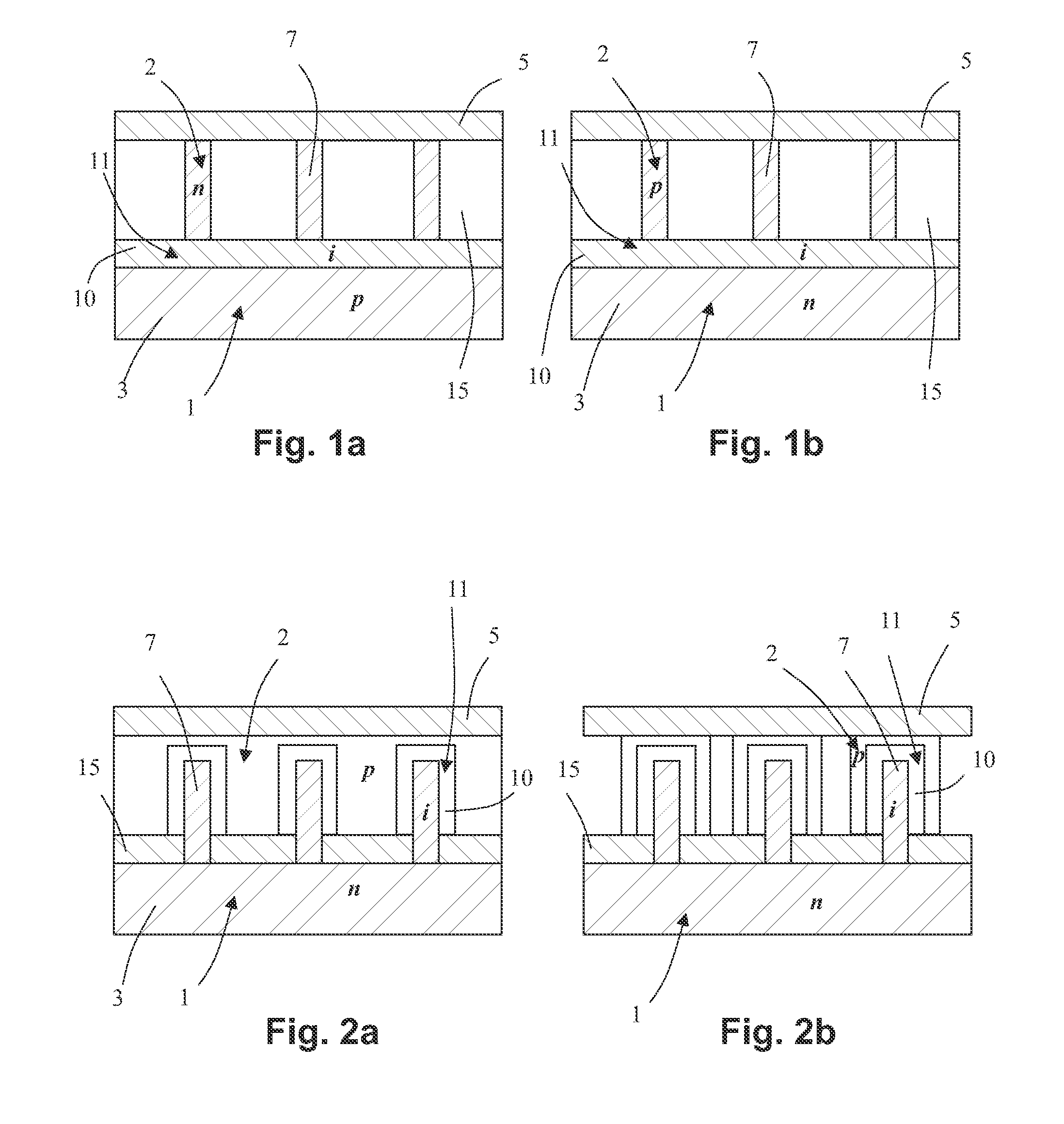
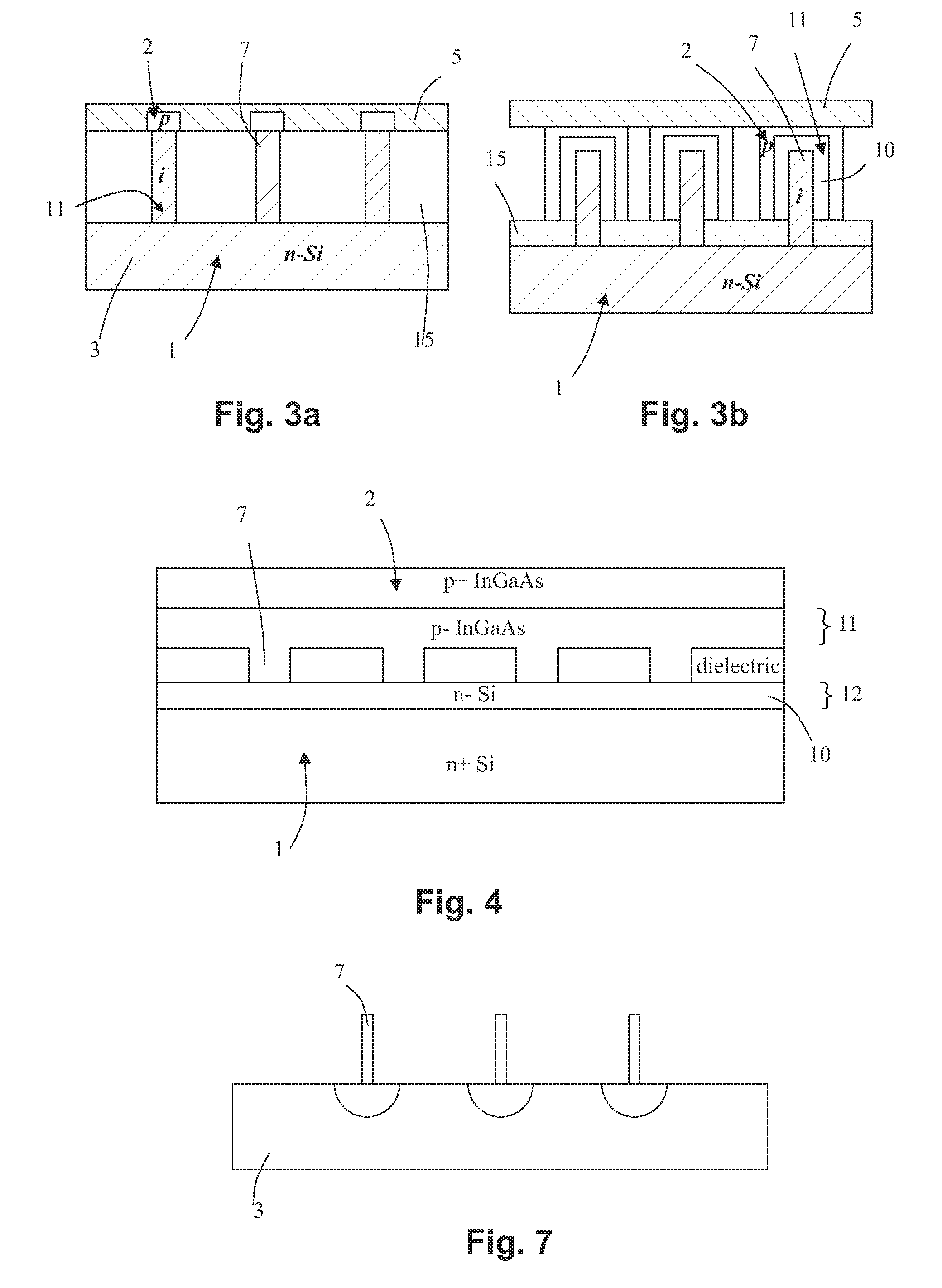
[0025]In the present invention one section of a semiconductor photodiode is partitioned by using a nanowire array comprising typically 1 to more than 10exp8) nanowires spaced apart from each other. Basically, the nanowires of the nanowire array connect the p and n regions of the photodiode to each other, whereby charge carriers, which are generated from absorbed light in a light absorption region, are due to a bias collected by the nanowires and efficiently conducted away. This can be used for different photodetectors and is in the following particular described for photodiodes (PD), avalanche photodiodes (APD), and separate absorption-multiplication avalanche photodiode (SAM APD).

[0026]For the purpose of this application the term nanowire is to be interpreted as a structure being essentially of nanometer dimensions in its width or diameter. Such structures are commonly also referred to as nanowhiskers, nanorods, etc. The basic process of nanowire formation on substrates by particle...


PUM


Abstract

The present invention provides a photodiode comprising a p-i-n or pn junction at least partly formed by first and second regions (2) made of semiconductor materials having opposite conductivity type, wherein the p-i-n or pn junction comprises a light absorption region (11) for generation of charge carriers from absorbed light. One section of the p-i-n or pn junction is comprises by one or more nanowires (7) that are spaced apart and arranged to collect charge carriers generated in the light absorption region (11). At least one low doped region (10) made of a low doped or intrinsic semiconductor material provided between the nanowires (7) and one of said first region (1) and said second region (2) enables custom made light absorption region and/or avalanche multiplication region of the active region (9).

Description

TECHNICAL FIELD OF THE INVENTION[0001]The present invention relates to photodiodes and avalanche photodiodes that includes nanowires as part of the pn or pin junction.BACKGROUND OF THE INVENTION[0002]A photodiode (PD) is a type of photodetector that is capable of generating charge carriers when exposed to light or other electromagnetic energy. An avalanche photodiode (APD) is another type of photodetector device that further to the charge carrier generation includes a multiplication of the charge carriers, i.e. an internal current gain effect, which enables a high sensitivity. Hereinafter PDs and APDs are commonly simply referred to as photodiodes when features common for both types of photodetectors are discussed.[0003]Semiconductor photodiodes fabricated using conventional planar technology comprise a vertical pn junction, i.e. a p-type semiconductor layer on an n-type semiconductor layer, or a vertical p-i-n junction, i.e. with one or more intermediate intrinsic or low doped semi...

Claims


Application Information

Patent Timeline
IPC IPC(8): H01L31/107B82Y15/00
CPCH01L31/03529Y02E10/50H01L31/105H01L31/1075H01L31/102H01L31/107
Inventor SAMUELSON, LARSCAPASSO, FEDERICOOHLSSON, JONAS
Owner QUNANO
Why Eureka
Try Eureka