Magnetron sputtering method, and magnetron sputtering apparatus

a sputtering apparatus and magnetron technology, applied in the direction of electrolysis components, vacuum evaporation coatings, coatings, etc., can solve the problems of low target utilization efficiency and poor uniformity of sputter film formation, and achieve efficient and uniform

Inactive Publication Date: 2011-08-04
TOKYO ELECTRON LTD +1
View PDF15 Cites 7 Cited by
  • Summary
  • Abstract
  • Description
  • Claims
  • Application Information

AI Technical Summary

Benefits of technology

[0052]According to the magnetron sputtering method and the magnetron sputtering apparatus of the present invention, due to the above structu

Problems solved by technology

In this case, if the leakage magnetic field formed on the target surface is stopped, only a region of the target surface facing the loop, th

Method used


Image

  • Magnetron sputtering method, and magnetron sputtering apparatus
  • Magnetron sputtering method, and magnetron sputtering apparatus
  • Magnetron sputtering method, and magnetron sputtering apparatus

Examples


embodiment 1

[0098](Embodiment 1)

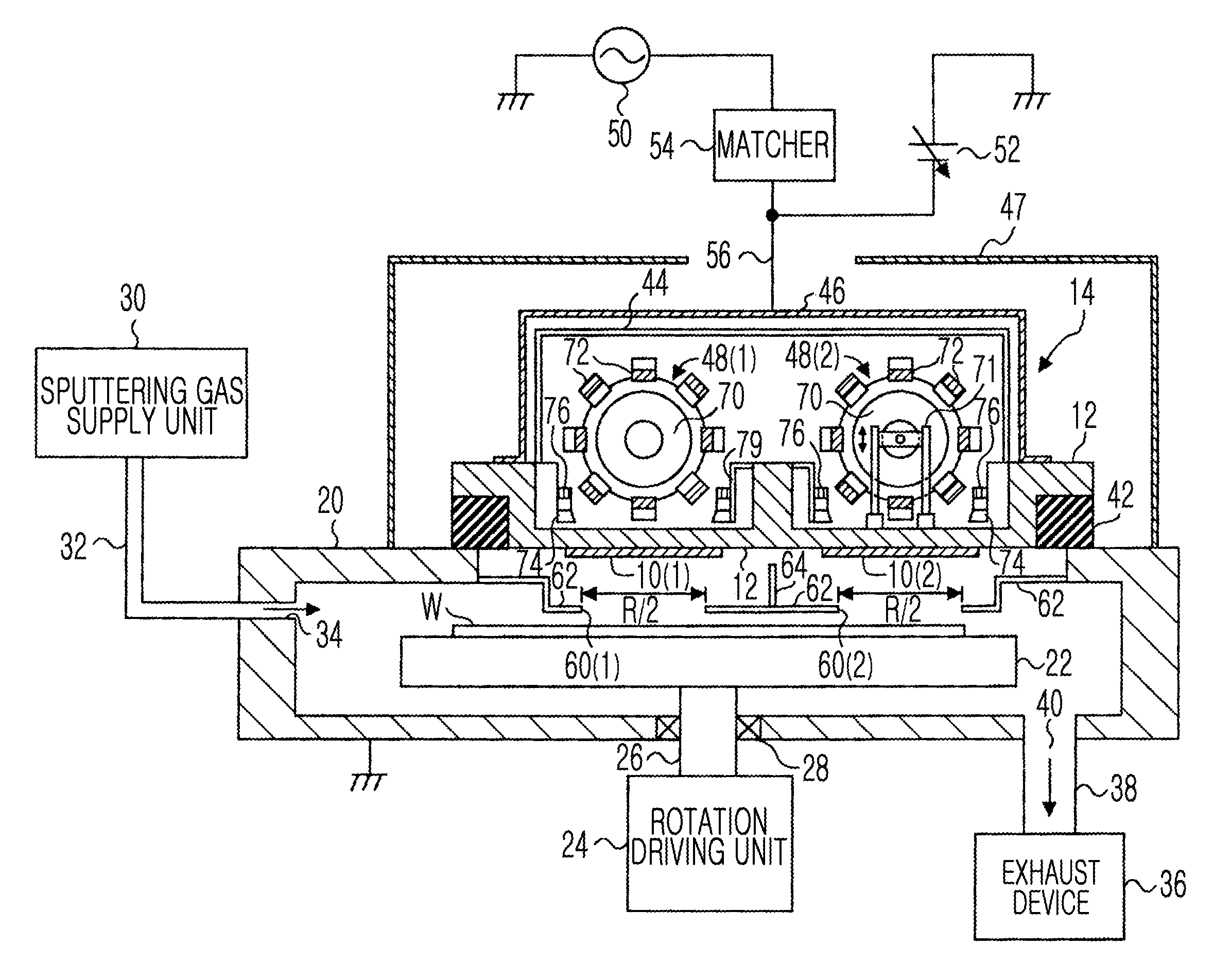
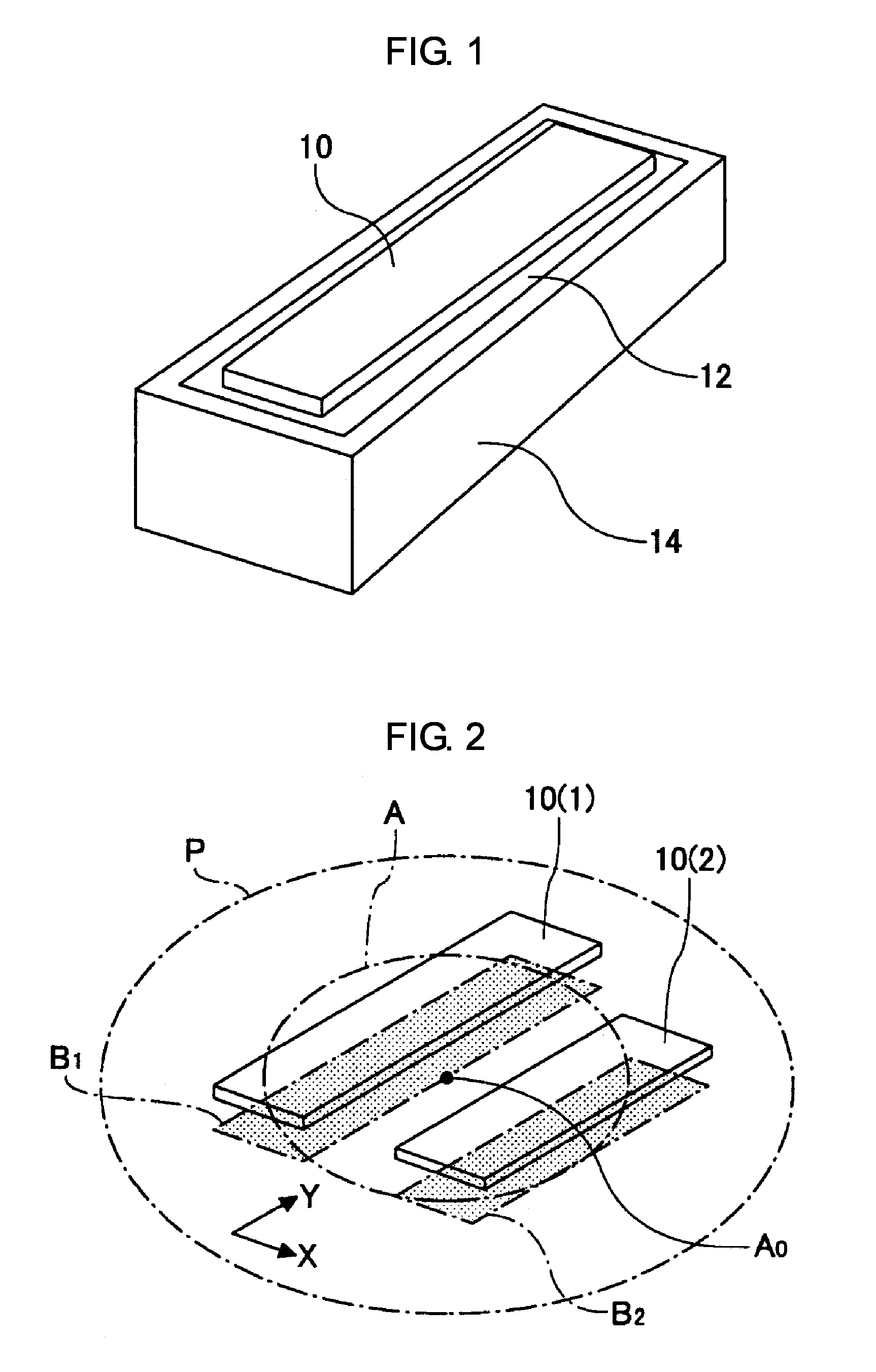
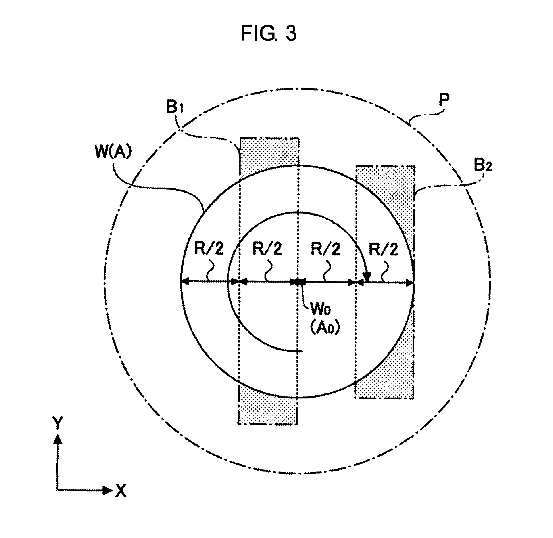
[0099]FIG. 3 shows a positional relationship between the wafer W and the portions A, B1, and B2 on the wafer arrangement surface P in Embodiment 1 of the present invention. In the present embodiment, the wafer W on which a film is to be deposited exactly overlaps with the circular reference region A on the wafer arrangement surface P. Also, the wafer W rotates at a predetermined rotation speed around the center Ao of the circular reference region A. Due to the rotation, a wafer central portion of the wafer W inner than a radius R / 2 is exposed to the sputtering particles from the thin and long target 10(1) only while the wafer central portion passes through the thin and long deposition region B1, and a wafer outer half region of the wafer W outer than the radius R / 2 is exposed to the sputtering particles from the thin and long targets 10(1) and 10(2) while the wafer outer half region passes through the thin and long deposition regions B1 and B2. Also, the wafer ce...

embodiment 2

[0112](Embodiment 2)

[0113]Next, Embodiment 2 of the present invention where requirements for a high degree of precision in a positional relationship between the rectangular targets 10(1) and 10(2) and the wafer W are relatively reduced when compared with Embodiment 1 will be explained.

[0114]Embodiment 2 is almost the same as Embodiment 1 except that the wafer W is disposed on the wafer arrangement surface P such that a center Wo of the wafer W is spaced apart by a predetermined distance a from the center Ao of the circular reference region A and the wafer W is rotated around the center Ao of the circular reference region A.

[0115]FIGS. 10 through 13 each show a positional relationship between the wafer W and the circular reference region A and the thin and long deposition regions B1 and B2 for every ¼)(90°-rotation of the wafer W in Embodiment 2.

[0116]FIG. 10 shows a positional relationship when the wafer W is most deviated in a +X direction (rightward in FIG. 10) due to the rotation...

embodiment 3

[0123](Embodiment 3)

[0124]Embodiment 3 of the present invention will now be explained with reference to FIGS. 16 through 18.

[0125]In Embodiment 3, as shown in FIG. 16, three thin and long deposition regions B1, B2, and B3 are set on the wafer arrangement surface P. The thin and long deposition regions B1, B2, and B3 are arranged in parallel at predetermined intervals in the X direction, and each cross the circular reference region A in the Y direction.

[0126]The thin and long deposition region B1 is disposed such that in a left region of the circular reference region A, a side in a +X direction (right side in FIG. 16) of the thin and long deposition region B1 passes through the center Ao of the circular reference region A. Also, the thin and long deposition region B3 is disposed such that in the left region of the circular reference region A, a side in a −X direction (left side in FIG. 16) of the thin and long deposition region B3 passes through edges of the circular reference region...


PUM

PropertyMeasurementUnit
Diameteraaaaaaaaaa
Diameteraaaaaaaaaa
Diameteraaaaaaaaaa

Abstract

A sputtering method includes disposing a plurality of thin and long deposition regions such that the thin and long deposition regions each cross in a first direction a circular reference region having a diameter equal to that of a semiconductor wafer, and are arranged at predetermined intervals in a second direction perpendicular to the first direction; disposing one of the plurality of thin and long deposition regions such that one side of sides thereof extending in the first direction passes through a substantial center of the circular reference region; disposing another of the plurality of thin and long deposition regions such that one side of sides thereof extending in the first direction passes through a substantial edge of the circular reference region; setting each of widths of the plurality of thin and long deposition regions such that a value obtained by summing the widths of the plurality of thin and long deposition regions in the second direction is substantially equal to a radius of the circular reference region; disposing a plurality of thin and long targets to face the corresponding thin and long deposition regions such that sputtering particles emitted from the plurality of thin and long targets are incident on the corresponding thin and long deposition regions; disposing a semiconductor wafer, while overlapping with the circular reference region; confining a plasma generated by a magnetron discharge in the vicinity of the targets, and emitting the sputtering particles from the targets; and rotating the semiconductor wafer at a predetermined rotation speed by using a normal line passing through the center of the circular reference region as a rotation central axis, to deposit a film on a surface of the semiconductor wafer.

Description

[0001]The present international application claims the benefit of Japanese Patent Application No. 2008-160991, filed on Jun. 19, 2008, in Japan Patent Office, and the disclosure of which is incorporated herein in its entirety by reference.TECHNICAL FIELD[0002]The present invention relates to a magnetron sputtering method that uses a magnetron discharge during a sputtering process, and more particularly, to a magnetron sputtering method and a magnetron sputtering apparatus that use a semiconductor wafer as an object to be processed.BACKGROUND ART[0003]In the manufacture of a semiconductor device, a process of forming a predetermined thin film on a semiconductor wafer and a process of patterning by lithography and etching the thin film are repeated several times. Sputtering methods, which are physical vapor deposition (PVD) methods where a target (a basic material for the thin film) is sputtered by ion bombardment and atoms of the target material are deposited onto a semiconductor waf...

Claims


Application Information

Patent Timeline
IPC IPC(8): C23C14/35
CPCC23C14/35H01J37/3423H01J37/3405
Inventor OHMI, TADAHIROGOTO, TETSUYASEKI, NOBUAKIKAWAKAMI, SATORUMATSUOKA, TAKAAKI
Owner TOKYO ELECTRON LTD
Why Eureka
Try Eureka