Substrate processing apparatus and method of manufacturing semiconductor device

a processing apparatus and semiconductor technology, applied in the direction of coatings, basic electric elements, chemical vapor deposition coatings, etc., can solve the problems of increasing the thermal budget of the substrate, increasing the resistivity, and taking longer to obtain a film, so as to achieve a higher film-forming rate, high production efficiency, and high quality

Active Publication Date: 2011-08-04
KOKUSA ELECTRIC CO LTD
View PDF30 Cites 159 Cited by
  • Summary
  • Abstract
  • Description
  • Claims
  • Application Information

AI Technical Summary

Benefits of technology

[0013]According to the present invention, a TiN film that is higher in quality than a TiN film formed by a conventional CVD method can be obtained at a higher film-forming rate, that is, with a higher productivity than a TiN film formed by an ALD method.

Problems solved by technology

However, when a film is formed using a CVD method, chlorine (Cl) tends to be easily absorbed into the film, compared to when a film is formed using an ALD method, resulting in an increase in resistivity, etc.
On the other hand, since a film-forming rate is slow, compared to when using the CVD method, it takes longer to obtain a film having a desired thickness, and a thermal budget of a substrate may be increased.
Also, productivity may be low due to the slow film-forming rate.

Method used


Image

  • Substrate processing apparatus and method of manufacturing semiconductor device
  • Substrate processing apparatus and method of manufacturing semiconductor device
  • Substrate processing apparatus and method of manufacturing semiconductor device

Examples


first embodiment

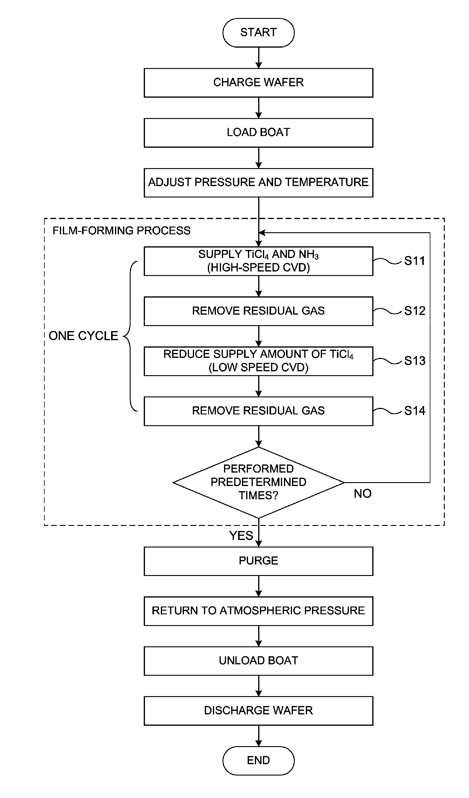
[0071]In this embodiment, a method of forming a TiN film as a conductive film on a substrate will be described. The TiN films are formed on the substrates through the first nozzle 410 and the second nozzle 420, which have different hole diameters, through two processes using a CVD method. First, as a first film-forming process, a TiN film is formed on the substrate by supplying a Ti-containing source through the gas supply hole 410a (the first nozzle 410) (step 1). Next, as a second film-forming process, a TiN film is formed on the substrate by supplying a Ti-containing source through the gas supply hole 420a (the second nozzle 420) having a smaller hole diameter than the gas supply hole 410a, which is achieved by supplying a sufficient supply amount of a nitride gas while relatively reducing a flow rate of the Ti-containing source compared to that of the nitride gas (step 2). A TiN layer is formed on the substrate by performing the first film-forming process and the second film-for...

second embodiment

[0094]Hereinafter, only parts different from those of the first embodiment will now be described in this embodiment.

[0095]In the first embodiment, the low-speed CVD method was used as the second film-forming process to reduce a supply amount of TiCl4 using the second nozzle 420 having a smaller hole diameter than the first nozzle 410 without flowing TiCl4 through the first nozzle 410 and simultaneously increase a supply amount of NH3. However, in this embodiment, TiCl4 flows through the first nozzle 410 in the second film-forming process. FIG. 7 depicts a sequence according to this embodiment. Also, FIG. 8 is a flowchart illustrating a process according to this embodiment. Hereinafter, the sequence according to this embodiment will be described with reference to FIGS. 7 and 8.

[0096](Step S21)

[0097]In step S21, in order to form a TiN film on the substrate using the high-speed CVD method as the first film-forming process, TiCl4 and NH3 flow at the same time under the same conditions a...

example 1

Gas Supply Example 1

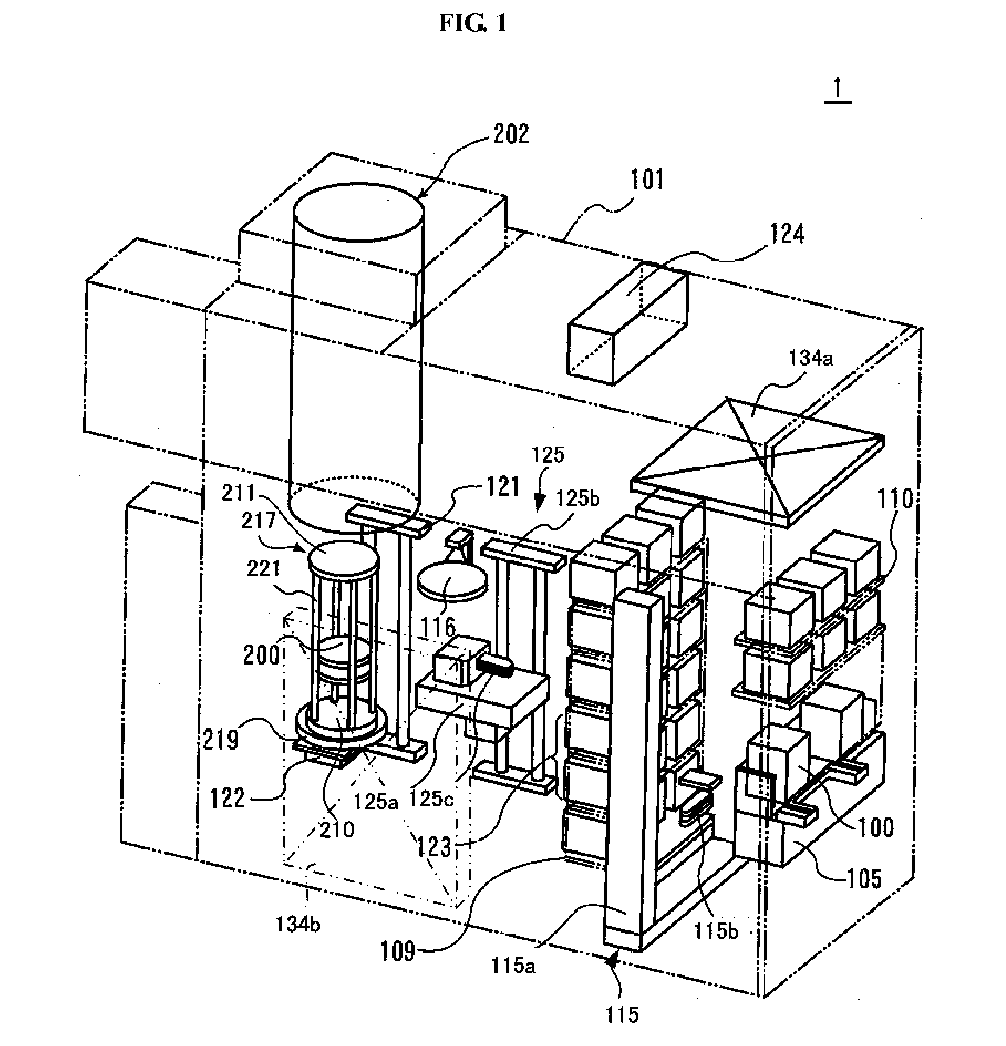
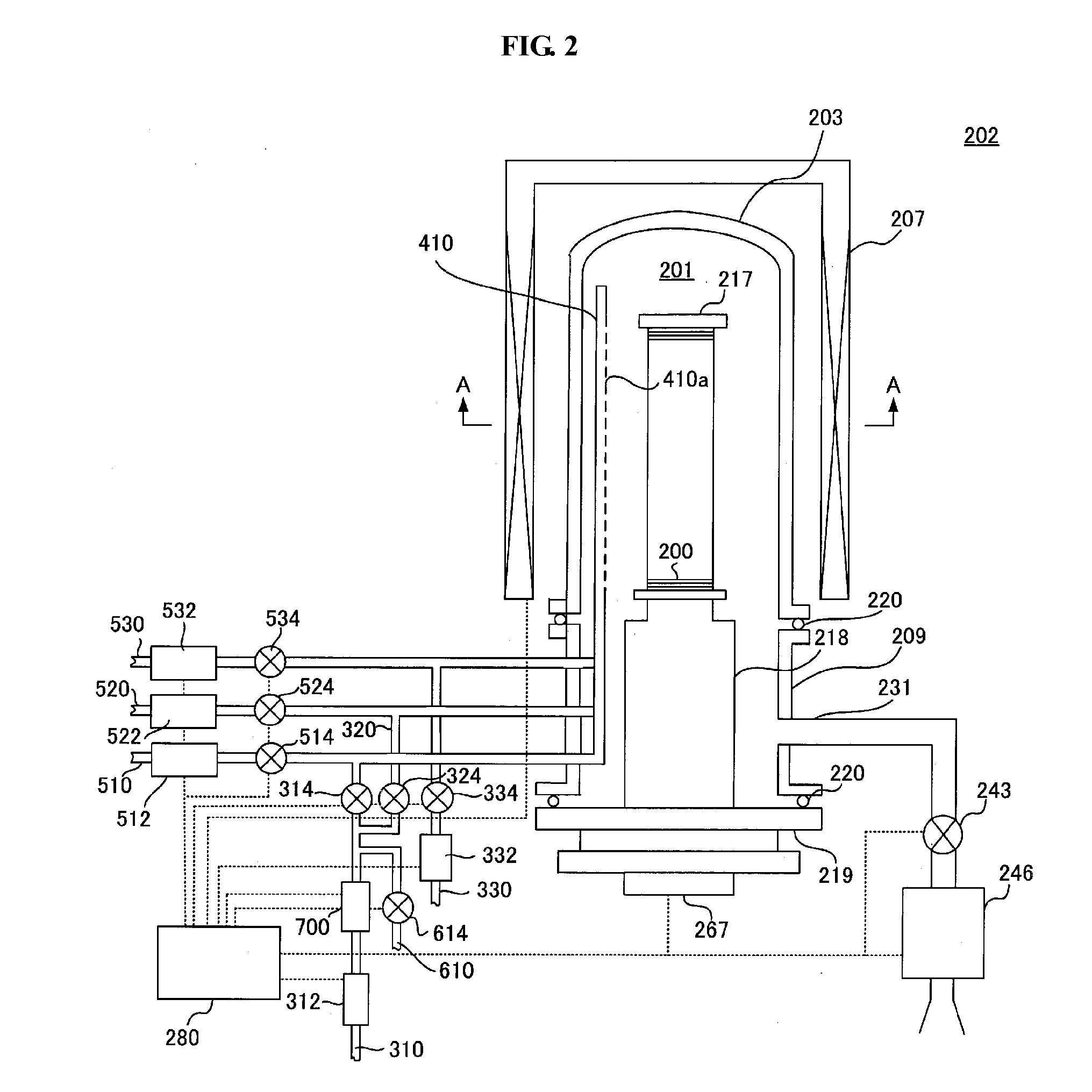
[0109]As shown in FIG. 11a, the first gas supply tube 310 for supplying the first processing gas (TiCl4) is connected to the first nozzle 410 via a valve vt1, the mass flow controller 312, a valve vt2 and a valve v1, which are arranged in order from an upstream side. Also, the first gas supply tube 310 is connected to the second gas supply tube 320 via the valve vt1, the mass flow controller 312 and the valve vt2, which are arranged in order from an upstream side, and is then connected to the second nozzle 420 via a valve v2. In addition, the carrier gas (N2) supply tube 510 (or 520) is connected to the first nozzle 410 via a valve vn1, the mass flow controller 512 or 522, a valve vn2 and the valve v1, which are arranged in order from an upstream side. Also, the carrier gas supply tube 510 (or 520) is branched from the valve vn1, the mass flow controller 512 (or 522) and the valve vn2, which are arranged in order from an upstream side, and is then connected to th...


PUM

PropertyMeasurementUnit
temperatureaaaaaaaaaa

Abstract

Provided are a substrate processing apparatus and a method of manufacturing a semiconductor device which are able to form a conductive film, which is dense, includes a low concentration of source-derived impurities and has low resistivity, at a higher film-forming rate. The substrate processing apparatus includes a processing chamber configured to stack and accommodate a plurality of substrates; a first processing gas supply system configured to supply a first processing gas into the processing chamber; a second processing gas supply system configured to supply a second processing gas into the processing chamber; and a control unit configured to control the first processing gas supply system and the second processing gas supply system. Here, at least one of the first processing gas supply system and the second processing gas supply system includes two nozzles which are vertically arranged in a stacking direction of the substrates and have different shapes, and the control unit is configured to supply at least one of the first processing gas and the second processing gas into the processing chamber through the two nozzles having different shapes when films are formed on the substrates by supplying the first processing gas and the second processing gas into the processing chamber at pulses having different film-forming rates.

Description

CROSS-REFERENCE TO RELATED PATENT APPLICATION[0001]This application claims priority to and the benefit of Japanese Patent Application No. 2010-018908 on Jan. 29, 2010 and 2010-278995 on Dec. 15, 2010, the disclosure of which is incorporated herein by reference.FIELD OF THE INVENTION[0002]The present invention relates to a substrate processing apparatus and a method of manufacturing a semiconductor device, and more particularly, to a substrate processing apparatus which forms a metal film or a metal compound on a substrate (a wafer) using a halogenated metal compound or an organometallic compound as a source, and a method of manufacturing a semiconductor device.DESCRIPTION OF THE RELATED ART[0003]Methods of forming a predetermined film on a substrate include a chemical vapor deposition (CVD) method. The CVD method is a method of forming a film including elements included in source molecules as components on a substrate through a reaction of at least two sources in a vapor phase or on...

Claims


Application Information

Patent Timeline
Patent Type & Authority Applications(United States)
IPC IPC(8): H01L23/482H01L21/00C23C16/455H01L21/3205
CPCH01L21/02186C23C16/45578C23C16/303C23C16/301C23C16/52C23C16/455H01L2924/0002H01L23/482H01L21/3205H01L21/00H01L2924/00C23C16/45546C23C16/45527H01L21/0228C23C16/45523C23C16/45561C23C16/45574H01L21/205
Inventor SAITO, TATSUYUKISAKAI, MASANORIKAGA, YUKINAOYOKOGAWA, TAKASHI
Owner KOKUSA ELECTRIC CO LTD
Why Eureka
Try Eureka