Capacitive touch sensor and fabrication method thereof and capacitive touch panel

a capacitive touch and capacitive technology, applied in the direction of converting sensor output electrically/magnetically, instruments, conductive pattern formation, etc., can solve the problems of high impedance, metal conducting line is liable to be broken at a junction point, and the line width cannot be narrowed to a great extent, so as to enhance the electrostatic protection of the capacitive touch panel, reduce the visibility, line impedance and parasitic capacitance of metallics

Inactive Publication Date: 2011-08-04
WINTEK CHINA TECH LTD +1
View PDF26 Cites 41 Cited by
  • Summary
  • Abstract
  • Description
  • Claims
  • Application Information

AI Technical Summary

Benefits of technology

[0005]The invention provides a capacitive touch sensor and a capacitive touch panel to reduce the visibility, line impedance and parasitic capacitance of metallic connecting lines between touch-sensing pads and enhance the electrostatic protection of the capacitive touch panel.
[0006]The invention provides a method for fabricating a capacitive touch sensor to effectively increase the production yield and material usage rate, and such fabrication method is also suitable for a plastic substrate.
[0009]In one embodiment, the metal printing line is a multi-layer stack printing structure and the area of each layer in the multi-layer stack printing structure is decreased from the bottom to the top of the multi-layer stack printing structure.
[0015]According to the design of the above embodiments, since the connecting line to connect two adjacent touch-sensing pads is a metal printing line formed by ink-jet printing, a very narrow connecting line is obtained to thereby reduce the visibility of the connecting line. Thus, the connecting line is not easily observed by a user and the visual effect is improved. In addition, since the line width is greatly decreased as a result of ink-jet printing, an overlapping area between the first metal printing line and the second printing line is significantly decreased to reduce the parasitic capacitance. Furthermore, the printing process may be used to form a multi-layer stack structure to increase the thickness of the metal traces. As the thickness is increased, the impedance is decreased to thereby increase the compatibility of different kinds of IC and reduce the probability of breakage. Besides, under the circumstance, the area to carry static currents is increased to improve electrostatic discharge (ESD) protection.
[0017]The above fabrication method can simplify processes and increase material usage rate and is suitable for a glass substrate as well as a plastic substrate.

Problems solved by technology

Though such disadvantage may be overcome by narrowing the line width, the line width cannot be narrowed to a great extent due to the limit on the fabrication process.
When the touch panel is subject to an antistatic test, the metal conducting line is liable to be broken at a junction point due to high impedance.
In addition, in case the metallic bridge structure and a metallic trace structure are formed by thin film deposition, photolithographic and etching, multiple processes are needed to hence increase the equipment cost and waste of materials.
Further, in case a plastic substrate is used as a transparent substrate, because the plastic substrate is typically not durable to ultraviolet light and acidic / alkaline solutions, the plastic substrate is liable to be damaged during the photolithographic and etching processes to result in a low production yield.

Method used


Image

  • Capacitive touch sensor and fabrication method thereof and capacitive touch panel
  • Capacitive touch sensor and fabrication method thereof and capacitive touch panel
  • Capacitive touch sensor and fabrication method thereof and capacitive touch panel

Examples


Embodiment Construction

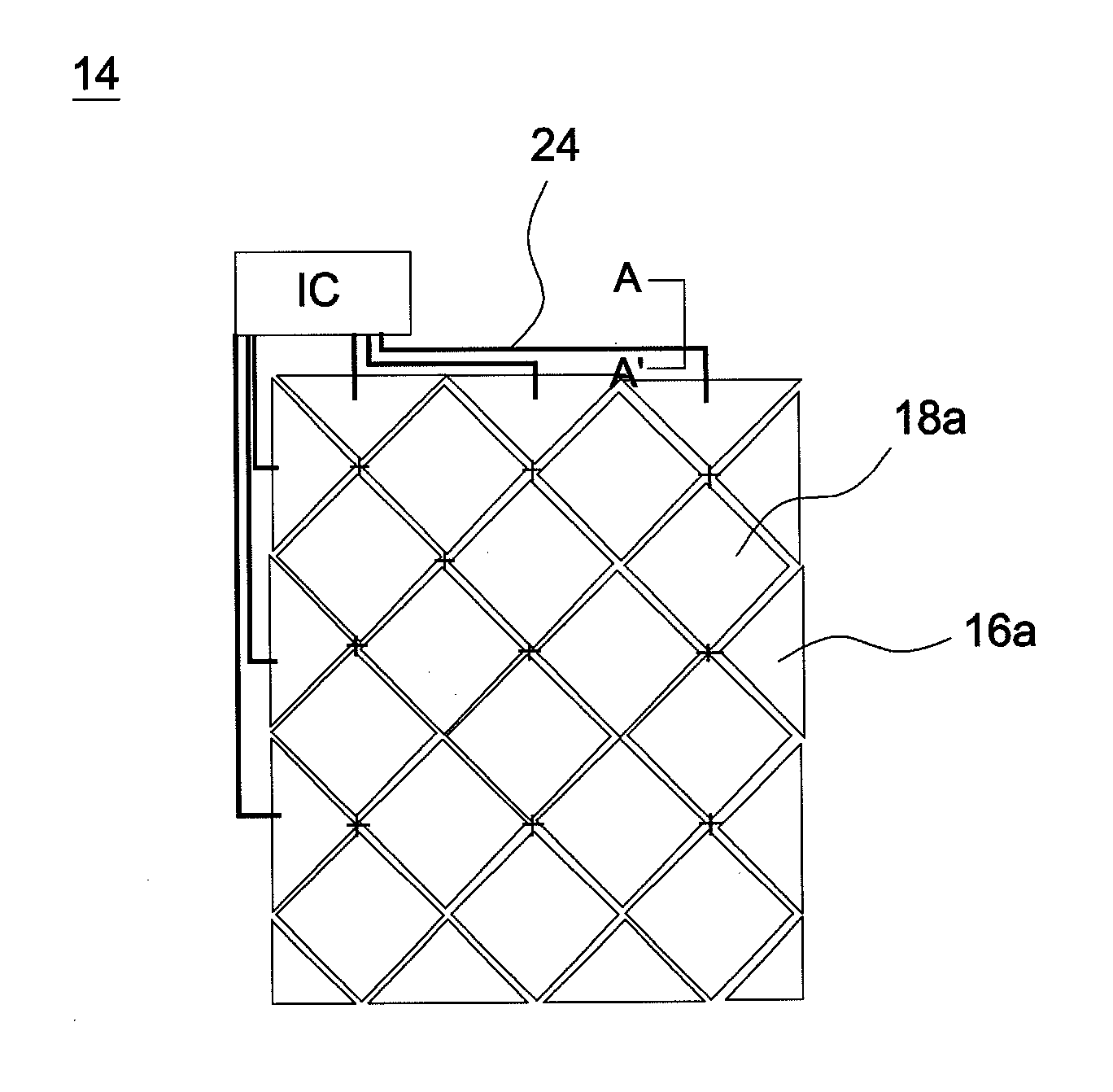
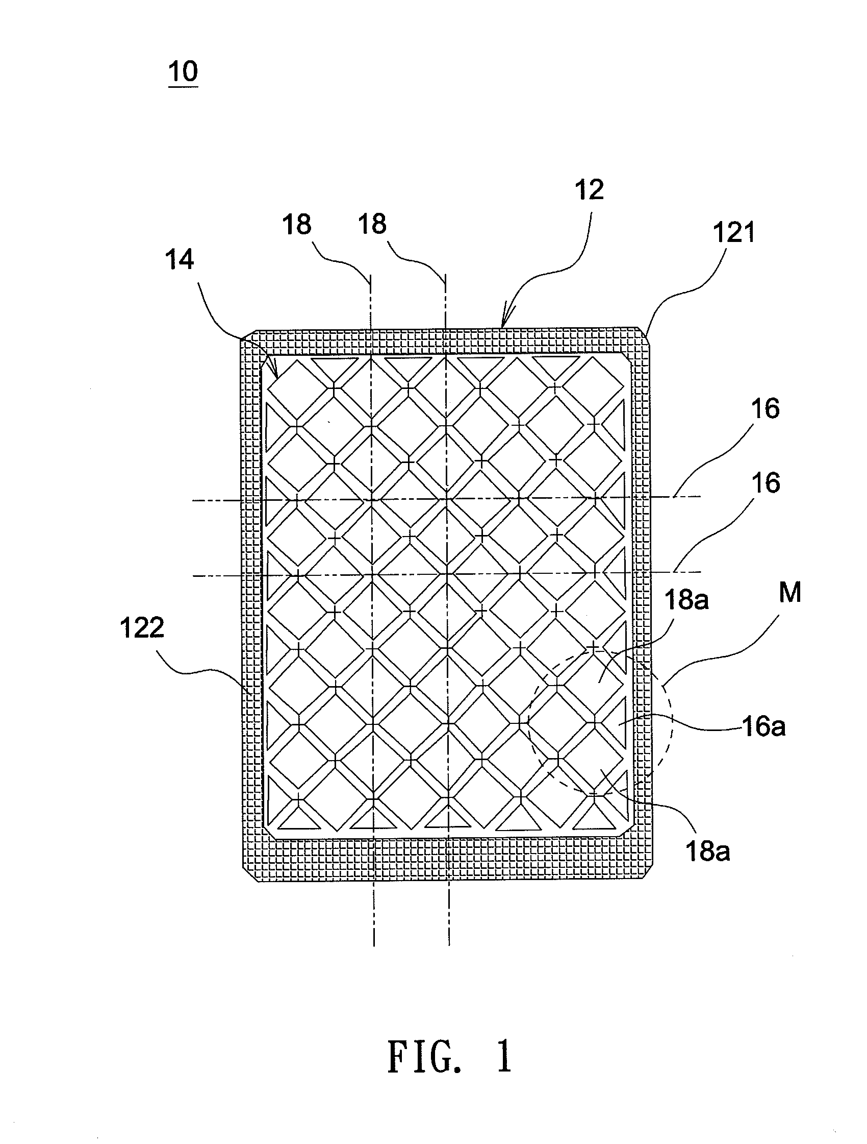
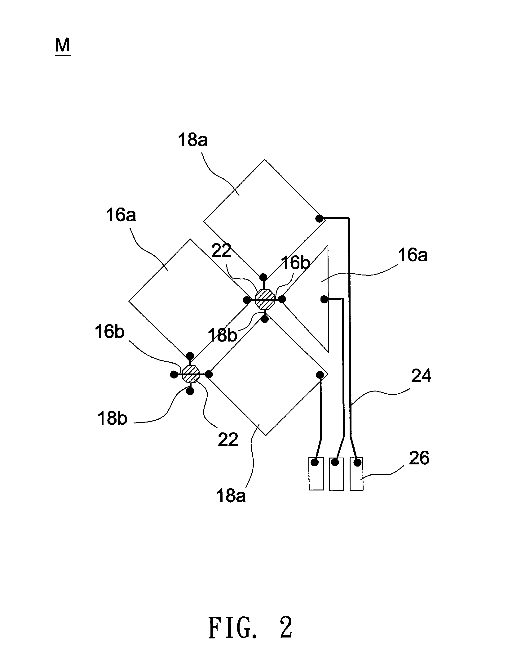
[0026]In the following detailed description of the preferred embodiments, reference is made to the accompanying drawings which form a part hereof, and in which are shown by way of illustration specific embodiments in which the invention can be practiced. In this regard, directional terminology, such as “top,”“bottom,”“front,”“back,” etc., is used with reference to the orientation of the Figure(s) being described. The components of the invention may be positioned in a number of different orientations. As such, the directional terminology is used for purposes of illustration and is in no way limiting. On the other hand, the drawings are only schematic and the sizes of components may be exaggerated for clarity. It is to be understood that other embodiments may be utilized and structural changes may be made without departing from the scope of the invention. Also, it is to be understood that the phraseology and terminology used herein are for the purpose of description and should not be ...


PUM

PropertyMeasurementUnit
widthaaaaaaaaaa
areaaaaaaaaaaa
transparentaaaaaaaaaa

Abstract

A capacitive touch sensor includes multiple first-axis traces, multiple second-axis traces, an insulation layer and multiple metal traces. Each first-axis trace includes multiple first touch-sensing pads and first connecting lines connected therebetween. Each second-axis trace includes multiple second touch-sensing pads and second connecting lines connected therebetween. At least one of the first connecting line and the second connecting line is a metal printing line.

Description

BACKGROUND OF THE INVENTION[0001]a. Field of the Invention[0002]The invention relates to a capacitive touch sensor, a method for fabricating a capacitive touch sensor, and a capacitive touch panel.[0003]b. Description of the Related Art[0004]In a conventional touch panel fabrication process, a metal line fabricated by a screen printing process or a photolithography process is highly visible for a user to influence visual effect. Though such disadvantage may be overcome by narrowing the line width, the line width cannot be narrowed to a great extent due to the limit on the fabrication process. Besides, a metallic bridge structure fabricated by a general photolithography process often has a film thickness of about 0.2 μm-0.3 μm. When the touch panel is subject to an antistatic test, the metal conducting line is liable to be broken at a junction point due to high impedance. In addition, in case the metallic bridge structure and a metallic trace structure are formed by thin film deposit...

Claims


Application Information

Patent Timeline
Patent Type & Authority Applications(United States)
IPC IPC(8): G06F3/044H05K3/10
CPCY10T29/49155G06F3/044G01D5/24H05K3/10G06F2203/04111G06F3/0445G06F3/0446
Inventor YIN, HSIANG-WEIWU, MING-KUNGSU, KUO-CHANGHUANG, PING-WEN
Owner WINTEK CHINA TECH LTD
Why Eureka
Try Eureka