CMOS image sensor

a technology of complementary oxide semiconductors and image sensors, applied in the field of metal complementary oxide semiconductor (cmos) image sensors, can solve the problems of high power consumption, low power consumption, complicated driving methods, etc., and achieve the effect of preventing charge sharing and preventing fixed pattern nois

Inactive Publication Date: 2011-08-11
SAMSUNG ELECTRO MECHANICS CO LTD +1
View PDF4 Cites 83 Cited by
  • Summary
  • Abstract
  • Description
  • Claims
  • Application Information

AI Technical Summary

Benefits of technology

[0014]Accordingly, the present invention has been made keeping in mind the above problems occurring in the prior art, and the present invention is intended to provide a CMOS image sensor which is capable of preventing the charge sharing caused when data stored in memory is read and the signal distortion caused by signal-dependent charge injection, and which is capable of preventing fixed pattern noise.
[0015]In order to accomplish the above object, the present invention provides a CMOS image sensor, including a pixel array including N unit pixels for converting optical signals, caused by light, into electric signals; a frame memory for eliminating offset voltage included in reset voltage and signal voltage transmitted from the pixel array and internal offset voltage, and performing Correlated Double Sampling (CDS) on the reset voltage and the signal voltage; and an analog-to-digital converter for converting an analog signal, transmitted from the frame memory, into a digital signal.

Problems solved by technology

Accordingly, the CCD image sensor has the advantages of excellent photosensitivity and reduced noise, but has the disadvantages of a complicated driving method and high power consumption because photocharges are successively transmitted.
Furthermore, a CMOS image sensor is disadvantageous in that noise generated in the form of voltage during transmission is combined with an output signal because electrons generated by light are converted into voltages for respective pixels and are then transmitted, but is advantageous in that power consumption is low and the level of integration can be increased compared to a CCD image sensor.
However, the conventional global shutter driving method of storing analog data in DRAM-type frame memory and using the analog data is problematic in that part of the quantity of the charge is lost because the charge of a capacitor is shared with the parasitic capacitance of a data line when a switch is turned on in order to read data, and is problematic in that a signal is distorted by signal-dependent charge injection which occurs when a switch is turned on or off.
In this case, fixed pattern noise may occur due to differences in the offset of the buffer.

Method used


Image

  • CMOS image sensor
  • CMOS image sensor
  • CMOS image sensor

Examples


Embodiment Construction

[0032]If in the specification, detailed descriptions of well-known functions or constructions may unnecessarily make the gist of the present invention obscure, the detailed descriptions will be omitted.

[0033]The terms and words used in the present specification and the accompanying claims should not be limitedly interpreted as having their common meanings or those found in dictionaries, but should be interpreted as having meanings adapted to the technical spirit of the present invention on the basis of the principle that an inventor can appropriately define the concepts of terms in order to best describe his or her invention.

[0034]It should be noted that the same reference numerals are used throughout the different drawings to designate the same or similar components as much as possible.

[0035]Preferred embodiments of the present invention will be described in detail below with reference to the accompanying drawings.

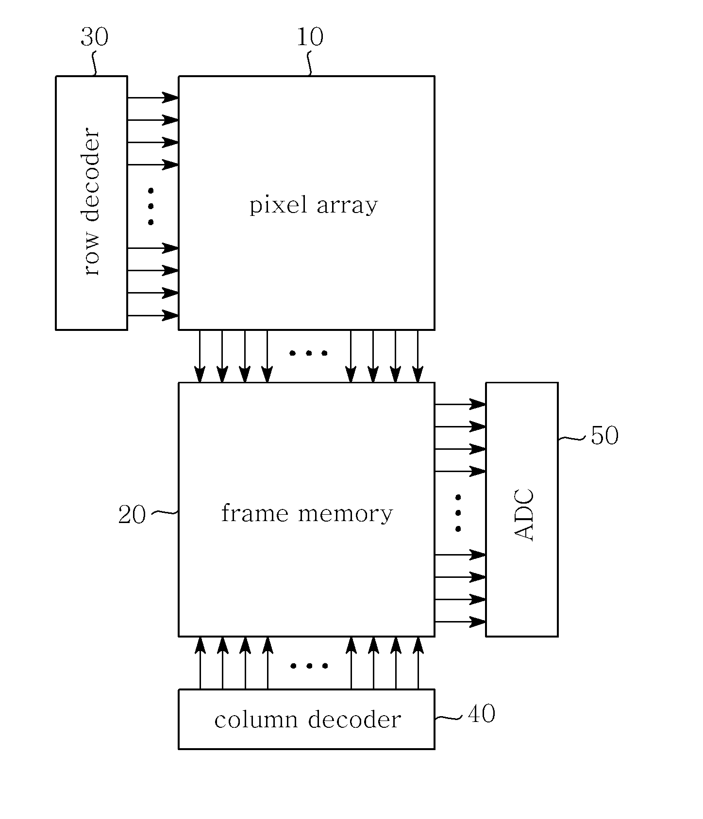
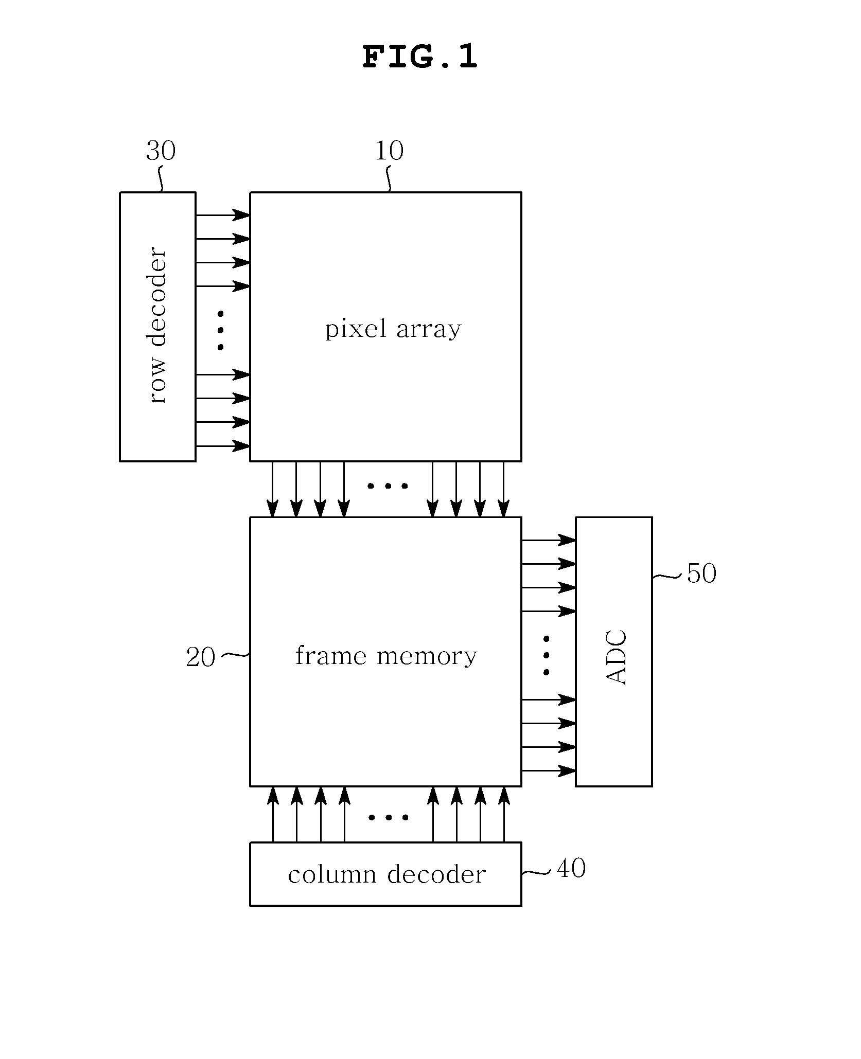
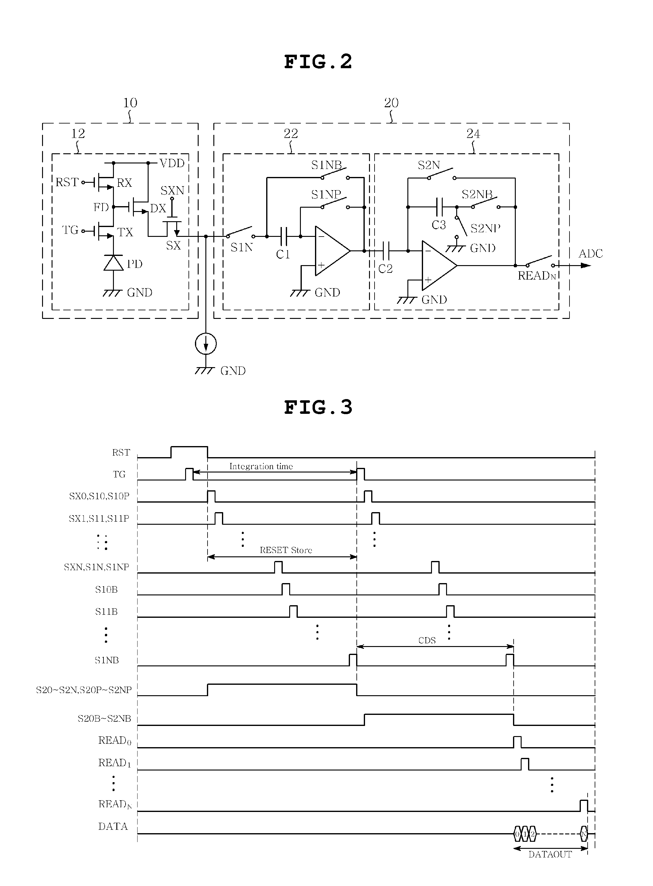
[0036]FIG. 1 is a diagram showing a CMOS image sensor according to a...


PUM


Abstract

Disclosed herein is a Complementary Metal-Oxide Semiconductor (CMOS) image sensor. The CMOS image sensor includes a pixel array, a frame memory, and an analog-to-digital converter. The pixel array includes N unit pixels for converting optical signals, caused by light, into electric signals. The frame memory eliminates offset voltage included in reset voltage and signal voltage transmitted from the pixel array and internal offset voltage, and performs Correlated Double Sampling (CDS) on the reset voltage and the signal voltage. The analog-to-digital converter converts an analog signal, transmitted from the frame memory, into a digital signal.

Description

CROSS REFERENCE TO RELATED APPLICATION[0001]This application claims the benefit of Korean Patent Application No. 10-2010-0011084, filed on Feb. 5, 2010, entitled “CMOS Image Sensor,” which is hereby incorporated by reference in its entirety into this application.BACKGROUND OF THE INVENTION[0002]1. Technical Field[0003]The present invention relates to Metal Complementary Oxide Semiconductor (CMOS) image sensors.[0004]2. Description of the Related Art[0005]In general, image sensors are installed in mobile phone cameras, digital still cameras, etc., and function to capture an image within the field of view, convert it into electric signals, convert the resulting image signals into digital signals and transmit the digital signals.[0006]Such image sensors are classified into Charge Coupled Device (CCD) image sensors and CMOS image sensors depending on the type of transmission.[0007]Specifically, a CCD image sensor transfers electrons, generated by light, to an output unit using gate puls...

Claims


Application Information

Patent Timeline
Patent Type & Authority Applications(United States)
IPC IPC(8): H04N5/335
CPCH04N5/3575H04N5/378H04N5/3745H04N25/616H04N25/77H04N25/75
Inventor KIM, BYUNG HOONBURM, JINWOOKCHOI, WON TAE
Owner SAMSUNG ELECTRO MECHANICS CO LTD
Why Eureka
Try Eureka