Reactive site deactivation against vapor deposition

a technology of reactive site and vapor deposition, which is applied in the direction of layered products, semiconductor/solid-state device details, coatings, etc., can solve the problems of increasing the pulse and purge time required to saturate the substrate surface, contaminating the substrate surface, and reducing the saturating effect of the substrate surfa

Active Publication Date: 2011-08-18
ASM IP HLDG BV
View PDF37 Cites 468 Cited by
  • Summary
  • Abstract
  • Description
  • Claims
  • Application Information

AI Technical Summary

Problems solved by technology

The film buildup can delaminate or flake from the reactor surfaces and contaminate the substrate surface.
Large amounts of loosely adhered film buildup on the reactor surfaces also increases the total surface area exposed to a reactant pulse, there

Method used


Image

  • Reactive site deactivation against vapor deposition
  • Reactive site deactivation against vapor deposition
  • Reactive site deactivation against vapor deposition

Examples


Embodiment Construction

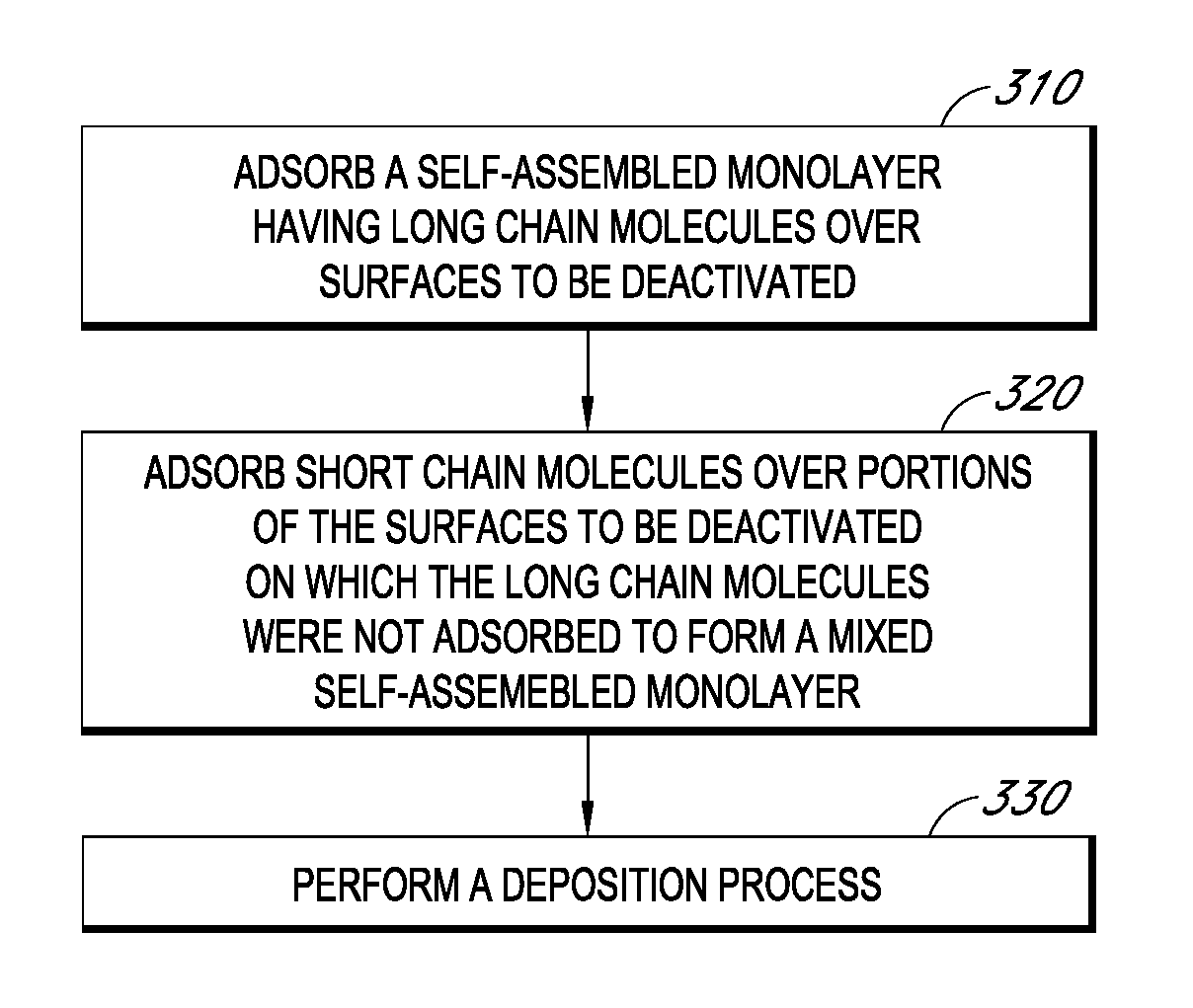
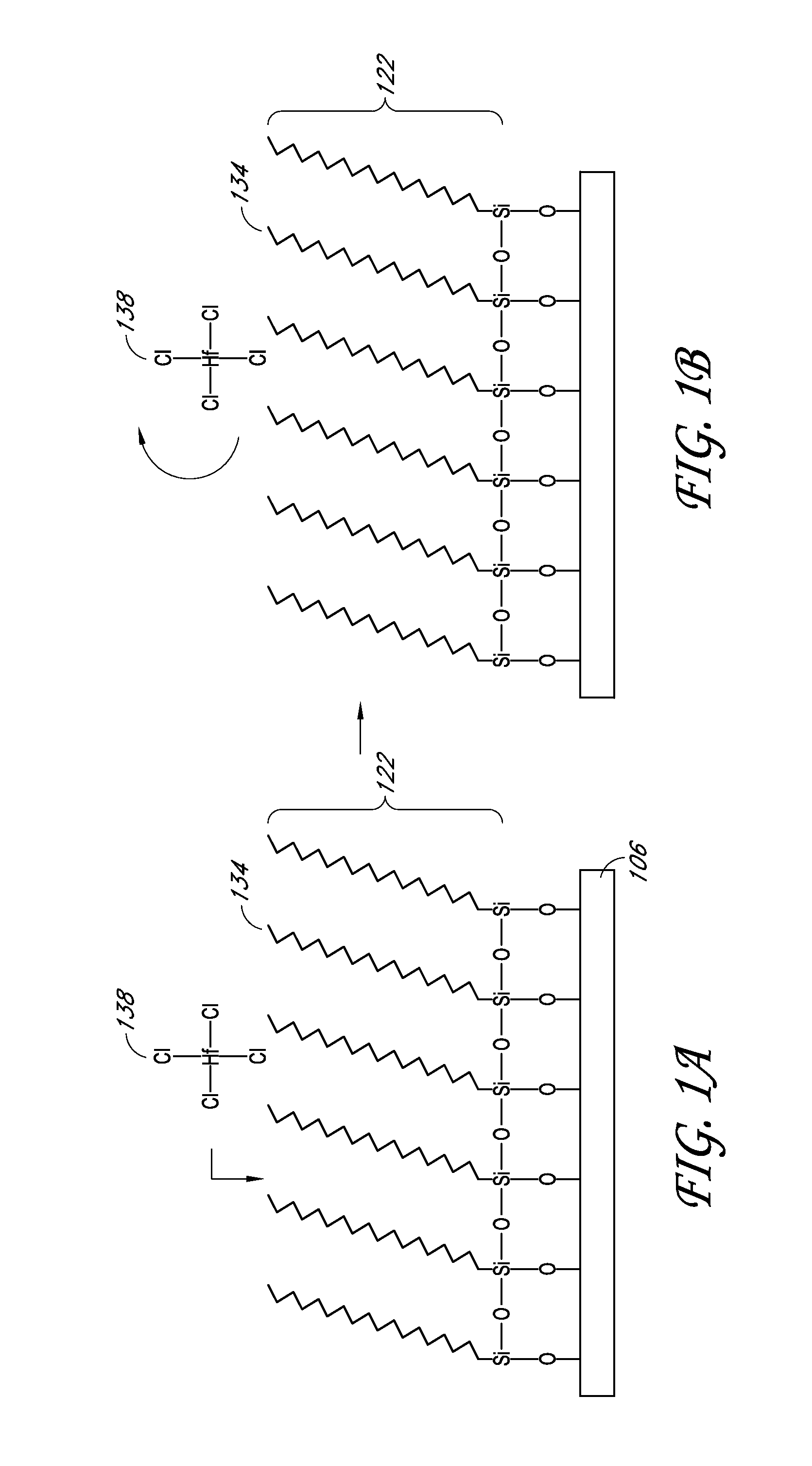
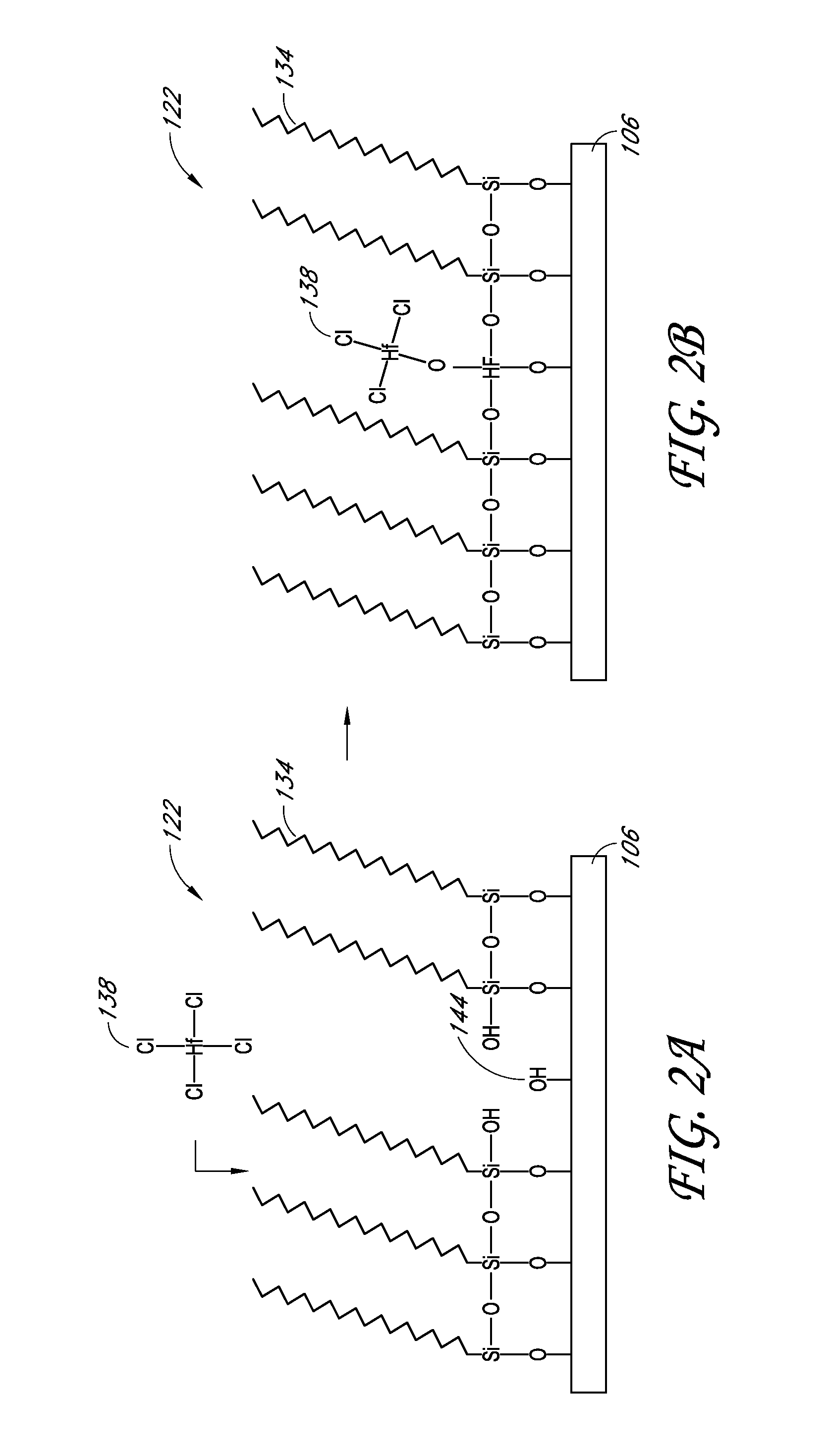
[0030]As noted in the Background section, processes exist to deactivate particular surfaces (e.g., reactor surfaces and surfaces of partially fabricated integrated circuit structures) against vapor deposition such as ALD to allow selective deposition on untreated surfaces. One such process involves forming a densely-packed, self-assembled monolayer (SAM) over exposed surfaces on which film deposition is not desired. A SAM is a relatively ordered assembly of molecules that spontaneously adsorb (also called chemisorb) from either vapor or liquid phase precursors on a surface. A typical SAM molecule includes a terminal functional group, a hydro-carbon chain and a head group. By forming a SAM over selected surfaces, the SAM can prevent film growth over the exposed surfaces using certain types of vapor precursors by blocking reactive sites on the exposed surface that would otherwise react with those deposition precursors. Such selective deactivation can be particularly effective against ...


PUM

PropertyMeasurementUnit
Fractionaaaaaaaaaa
Fractionaaaaaaaaaa
Timeaaaaaaaaaa

Abstract

Methods and structures relating to the formation of mixed SAMs for preventing undesirable growth or nucleation on exposed surfaces inside a reactor are described. A mixed SAM can be formed on surfaces for which nucleation is not desired by introducing a first SAM precursor having molecules of a first length and a second SAM precursor having molecules of a second length shorter than the first. Examples of exposed surfaces for which a mixed SAM can be provided over include reactor surfaces and select surfaces of integrated circuit structures, such as insulator and dielectric layers.

Description

BACKGROUND[0001]1. Field of the Invention[0002]This application relates generally to inhibiting vapor deposition on selected surfaces, such as reactor surfaces or select surfaces on a substrate.[0003]2. Description of the Related Art[0004]Atomic layer deposition (ALD) is a known process in the semiconductor industry for forming thin films of materials on substrates, such as silicon wafers. ALD is a type of vapor deposition wherein a film is built up through self-saturating surface reactions performed in cycles. In an ALD process, gaseous precursors are supplied, alternatingly and repeatedly, to the substrate to form a thin film of material on the substrate. One reactant adsorbs in a self-limiting process on the wafer. A subsequent reactant pulse reacts with the adsorbed material to form a molecular layer of the desired material. The subsequent pulse can reduce or getter ligands from the adsorbed layer, can replace such ligands or otherwise add atoms (e.g., oxidize, nitridize, etc.)....

Claims


Application Information

Patent Timeline
IPC IPC(8): H01L29/00B05D1/36H01L21/302C23C16/04B32B43/00C23C16/00C23F1/00
CPCB05D1/32B05D1/60B05D5/08B82Y30/00C23C16/04H01L29/517H01L21/02181H01L21/0228H01L21/02304H01L21/28194C23C16/45525H01L21/76826H01L21/76834H01L21/205
Inventor SHERO, ERICVERGHESE, MOHITHMUSCAT, ANTHONYMILLER, SHAWN
Owner ASM IP HLDG BV
Why Eureka
Try Eureka