Nonvolatile semiconductor memory device
a semiconductor memory and non-volatile technology, applied in static storage, digital storage, instruments, etc., can solve the problems of unable to perform normal sense operation, different limitations of flash memory, etc., to achieve stable sensing, high speed, and satisfy rapidity and readout accuracy.
- Summary
- Abstract
- Description
- Claims
- Application Information
AI Technical Summary
Benefits of technology
Problems solved by technology
Method used
Image
Examples
first embodiment
[Memory Cell Configuration]
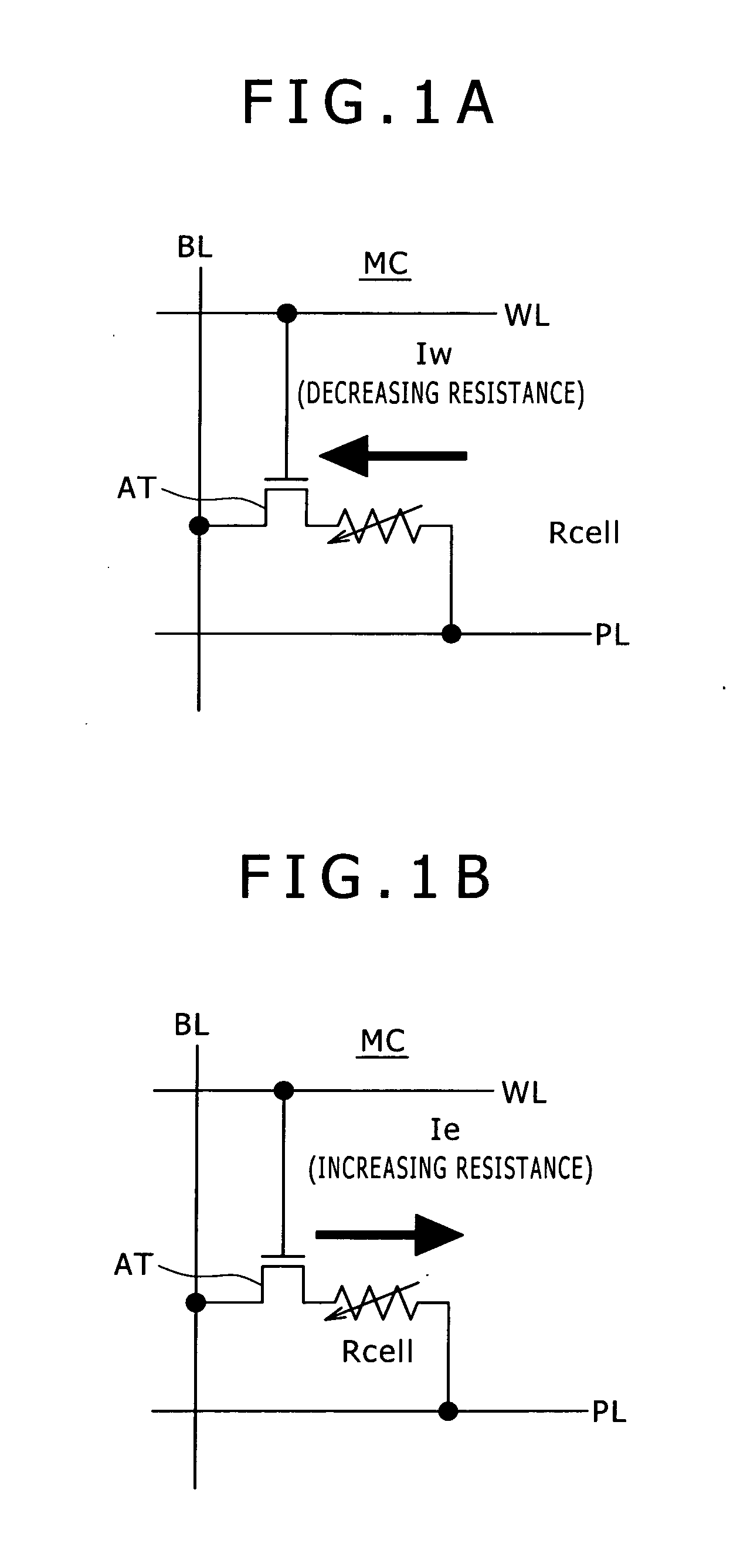
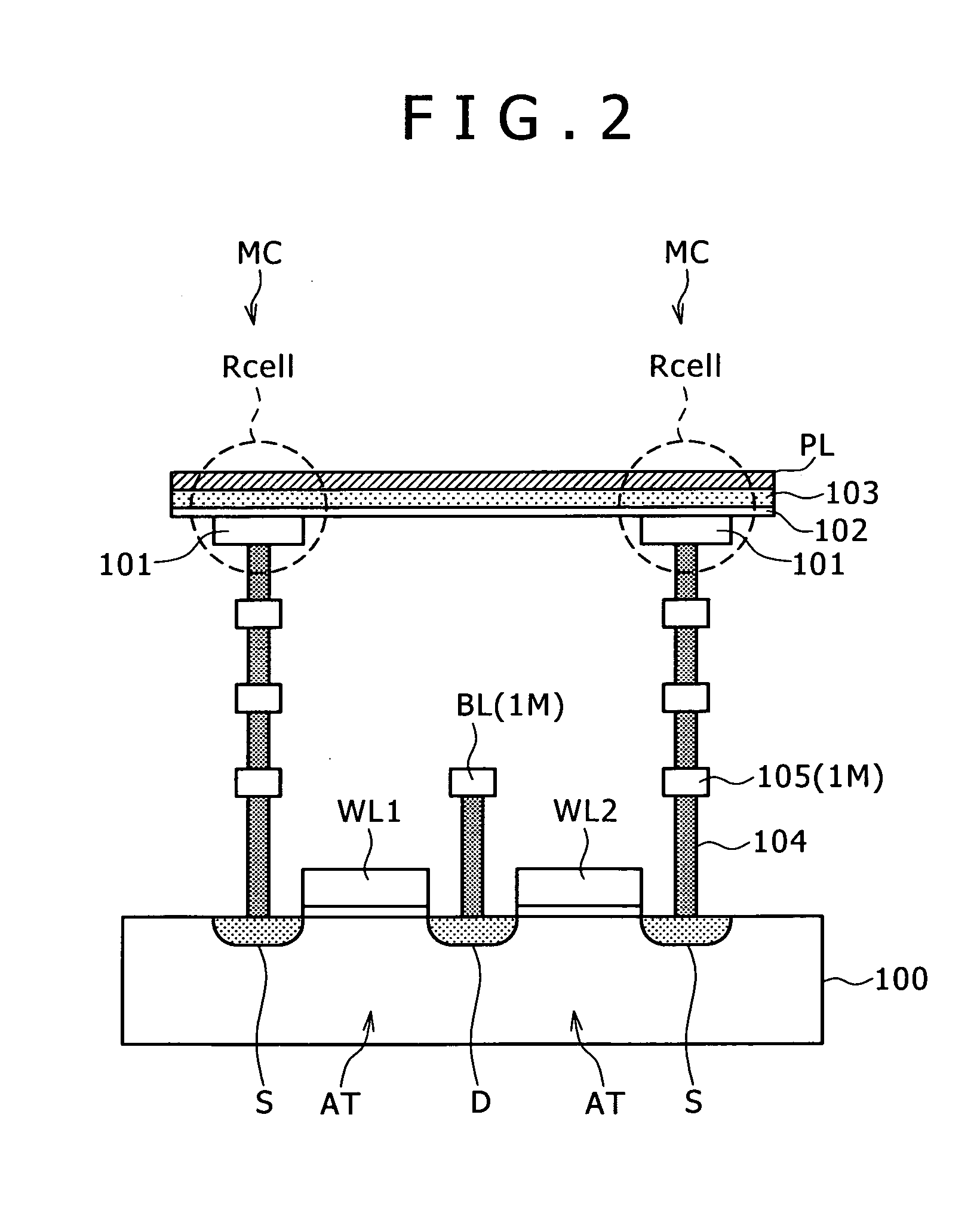
[0072]FIG. 1A and FIG. 1B are diagrams of an equivalent circuit of a memory cell common to embodiments of the present invention. Incidentally, while FIG. 1A shows the direction of a writing current Iw, and FIG. 1B shows the direction of an erasing current Ie, the configuration of the memory cell itself is common to both diagrams.
[0073]The memory cell MC illustrated in FIGS. 1A and 1B has one memory cell resistance Rcell as the “variable cell resistance Rcell” and one access transistor AT.
[0074]One terminal of the memory cell resistance Rcell is connected to a plate line PL. Another terminal of the memory cell resistance Rcell is connected to the source of the access transistor AT. The drain of the access transistor AT is connected to a bit line BL. The gate of the access transistor AT is connected to a word line WL as an “access line.”
[0075]Incidentally, while the bit line BL and the plate line PL are orthogonal to each other in FIGS. 1A and 1B, the bit li...
second embodiment
[0183]The present embodiment and subsequent embodiments represent modifications of circuit configurations of the sense amplifier and the like. Thus, a general configuration, circuits and block configurations other than those related to the modifications, and the basics of operation are similar to those of the first embodiment. Description will therefore be made centering on the modifications.
[0184]FIG. 14 is a schematic diagram of a column circuit configuration according to the present embodiment. FIGS. 15A to 17C2 show control waveforms and timing of a dynamic read, a static read, and a hybrid read.
[0185]Supplied pulses are determined so as to correspond to reversed conductivity types of main transistors (FIG. 15A, FIG. 15B, FIG. 16A, FIG. 16B, FIG. 17A, and FIG. 17B). In addition, inverted signals (high active signals) of the first load control signal ( / DC) and the precharge signal ( / PRE), which inverted signals are denoted with “ / ” removed, are supplied from a control circuit 11 ...
third embodiment
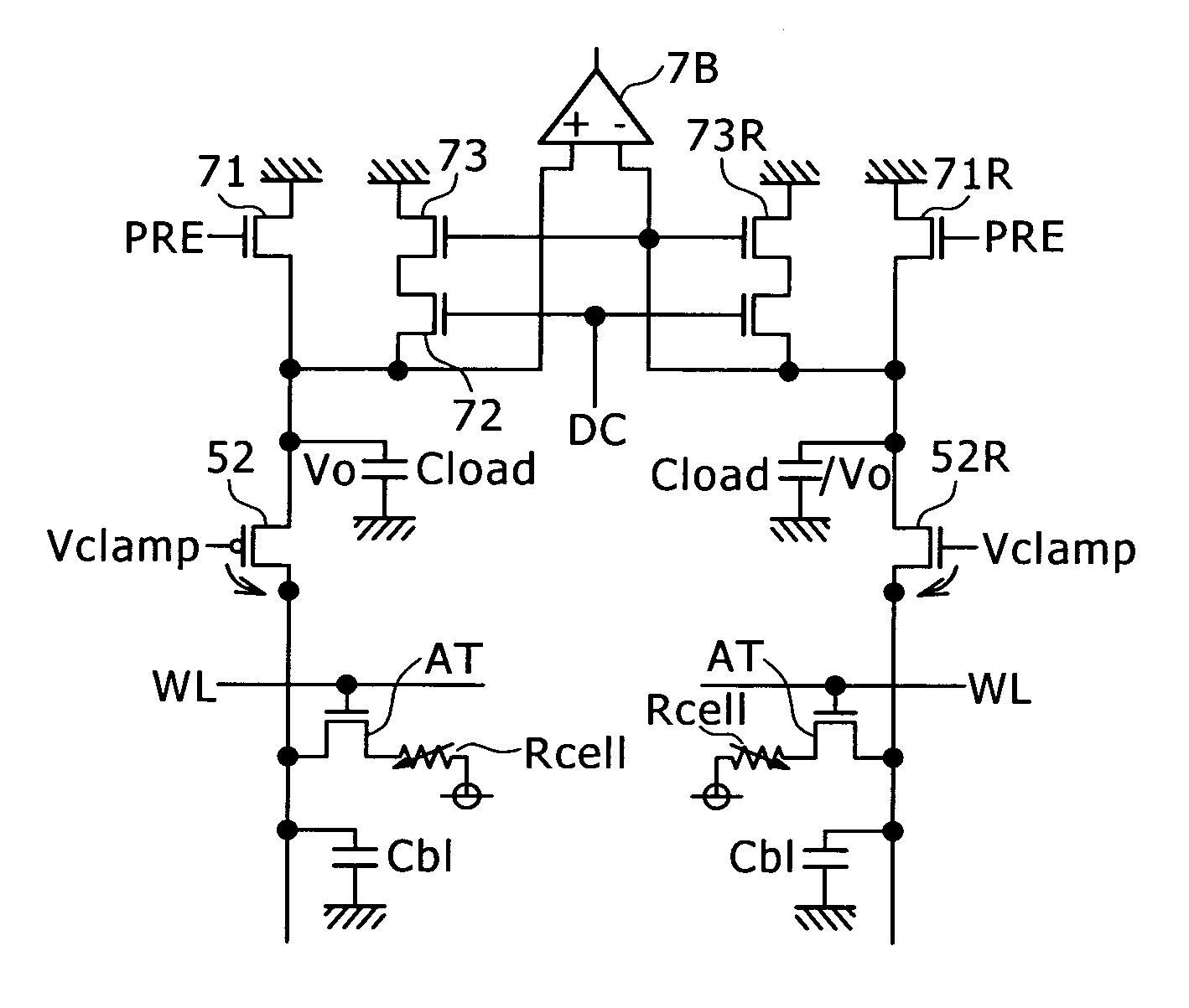
[0187]FIG. 18 is a schematic diagram of a column circuit configuration according to a third embodiment. FIGS. 19A to 21C2 show control waveforms and timing of a dynamic read, a static read, and a hybrid read.
[0188]The circuit configuration shown in FIG. 18 is different from that of FIG. 9 in that a voltage applied to a plate line PL connected to a variable cell resistance Rcell is a readout BL voltage VR (>0), and in that a voltage line connected to a precharge transistor 71 is conversely a GND voltage supply line. That is, the direction of a cell current is reversed. In addition, the precharge transistor 71 and a first control switch 72 are changed from a PMOS transistor to an NMOS transistor, and a load separating switch 52 is changed from an NMOS transistor to a PMOS transistor. The orientation of a current source connected to the first control switch 72 (direction of a current made to flow) is also reversed.
[0189]The other configuration on a memory cell side in FIG. 18 is simila...
PUM
 Abstract
Description
Claims
Application Information


