Process for making an electric testing of electronic devices

Active Publication Date: 2011-08-18
STMICROELECTRONICS SRL
View PDF16 Cites 22 Cited by
  • Summary
  • Abstract
  • Description
  • Claims
  • Application Information

AI Technical Summary

Benefits of technology

[0030]Moreover the testing of a specific device is very often linked to the particular type of used ATE and to the specific characteristics of its test resources, and thus it would be suitable to find such a new standard ap

Problems solved by technology

However, the disadvantages of this type of methodology are multiple.
In particular, the testing of complex devices on wafer using this type of methodology is very complicated since more testing operations are executed and thus to contact the wafer more times.
Moreover, the use of probes that connect the ATE to the wafer often implies the damaging of the pads of the selected devices, complicating the successive assembly of the devices themselves.
Moreover, making the testing of more devices connected in parallel requires the use of probe cards with a very high number of probes, increasing the problems of contacting and, thus, of electric continuity between the probes of the probe card and the pads of the DUT and causing also problems of electric performance loss.
It is also to be said that the number of resources of the ATE to be used increases according to the number of pads to be contacted on the DUT to be tested and, in consequence, the number of DUT that

Method used


Image

  • Process for making an electric testing of electronic devices
  • Process for making an electric testing of electronic devices
  • Process for making an electric testing of electronic devices

Examples


Example

[0190]With reference to these figures, the steps are now described of a process of electric testing of electronic devices according to one embodiment. In particular, as it will be clear hereafter in the description, one embodiment describes a testing process of the supervised type.

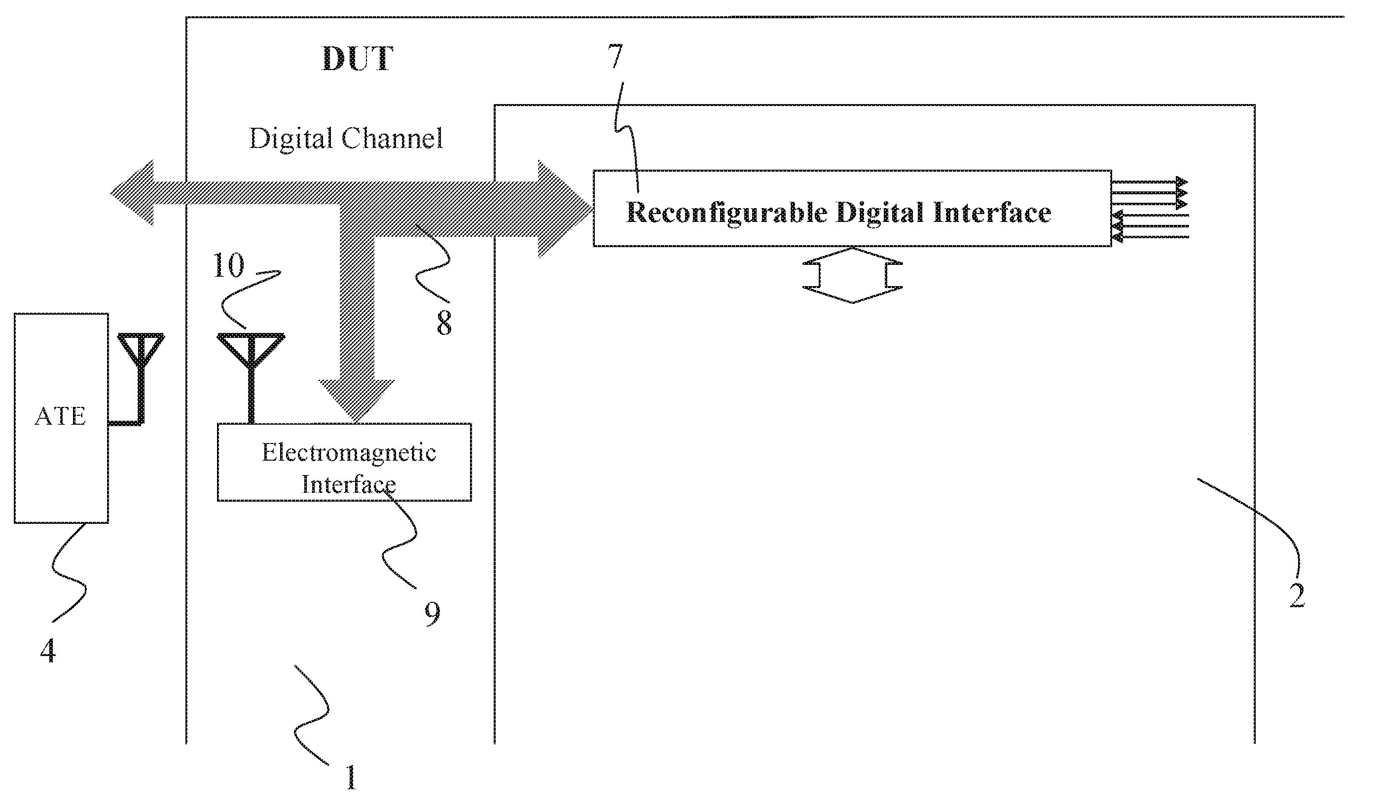
[0191]In particular, FIG. 4 shows a schematic representation of a digital ATE 4 connected to the device DUT 1 wherein a reconfigurable digital interface RDI 7 is integrated suitable for creating, between the DUT 1 and the digital ATE 4, a mainly digital communication channel ChD 8 that, advantageously, can comprise multiple wired or wireless, or in part wired and in part wireless, communication lines. In particular, at least one part of the digital channel (and at most the whole digital channel) of the digital interface RDI 7 of the DUT 1, indicated with 8 in the figure, instead of being connected directly to the ATE 4, is connected to at least one further wireless or wireline interface. According to the e...


PUM


Abstract

The disclosure relates to a process for making an electric testing of electronic devices DUT, of the type comprising the steps of: connecting at least one electronic device DUT to an automatic testing apparatus or ATE apparatus suitable for making the testing of digital circuits; sending, through said ATE apparatus, control signals for the electric testing to said electronic device DUT. Advantageously, the process also comprises the steps of: making the electric testing of said electronic device DUT through at least one reconfigurable digital interface RDI connected to said ATE apparatus through a dedicated digital communication channel and comprising a limited number of communication or connection lines strictly appointed to the exchange of the testing information; and sending from said electronic device DUT to said ATE apparatus response messages, if any, containing measures, failure information and data in response to said control signals and through said digital communication channel.

Description

BACKGROUND[0001]1. Technical Field[0002]The present disclosure relates to a process for making an electric testing of electronic devices.[0003]The present disclosure also relates to a system for making the electric testing of electronic devices.[0004]The present disclosure also relates to a reconfigurable digital interface for making the electric testing of electronic devices.[0005]The disclosure particularly, but not exclusively, relates to a process for making an electric testing of electronic devices, of the type comprising at least one wafer electric selection step chosen among: for example a testing of the electric type on wafer or Electrical Wafer Sort (EWS) or of the Final Test type or even testing of incorporated devices System in Package (SiP), or testing of the Wafer Level Burn-In (WLBI) type too, made under stress and when the temperature varies, or again testing of complex electronic systems, and the following description is made with reference to this field of applicati...

Claims


Application Information

Patent Timeline
IPC IPC(8): G06F11/00
CPCG01R31/3025G01R31/31908G01R31/318572H01L2224/16145H01L2224/32145H01L2224/32225H01L2224/48091H01L2224/73265H01L2924/15311H01L2924/13091H01L2924/00014H01L2924/00
Inventor PAGANI, ALBERTO
Owner STMICROELECTRONICS SRL
Why Eureka
Try Eureka