Method for manufacturing semiconductor device

Active Publication Date: 2011-08-25
KIOXIA CORP +1
View PDF9 Cites 27 Cited by
  • Summary
  • Abstract
  • Description
  • Claims
  • Application Information

AI Technical Summary

Benefits of technology

[0025]According to the present invention, the removal of a deposited film and polishing of silicon in a peripheral portion of a device substrate are carried out by using a polishing tape. Compared to the use of a diamond disk or the like, the use of a polishing tape allows the tape to make soft contact with a polishing object, preventing a crack or defect in a device substrate. Further, the use of a polishing tape makes it possible to polish a silicon substrate in a wet environment. For example, polishing of a device substrate can be carried out while covering a surface of a deposited film, covering device interconnects, with water. Such wet polishing can prevent foreign matter or contaminants from adhering to a surface of a deposited film. In the case of polishing with the use of a diamond disk, fall or wear of diamond abrasive particles will occur during long-term use of the diamond disk. In the cas

Problems solved by technology

The positional control of such a polishing machine is fairly cumbersome.
Further, a surface of a deposited film, e.g., covering device interconnects, of a silicon substrate is likely to be stained.
In addition, when a high contact pressure of a diamond disk on a silicon substrate is used in order to ensure an appropriately high polishing rate, the large pressure can cause significant damage, such as crack, to the silicon substrate.
The use of a low contact pressure to prevent this problem will lead to a considerably low removal rate for a deposited film and silicon.
This requires high-precision positioning of the grinding stone and necessitates a special structure for that, making the apparatus construction complicated.
On the other hand, when the removal of a

Method used


Image

  • Method for manufacturing semiconductor device
  • Method for manufacturing semiconductor device
  • Method for manufacturing semiconductor device

Examples


Embodiment Construction

[0037]Preferred embodiments of the present invention will now be described in detail with reference to the drawings.

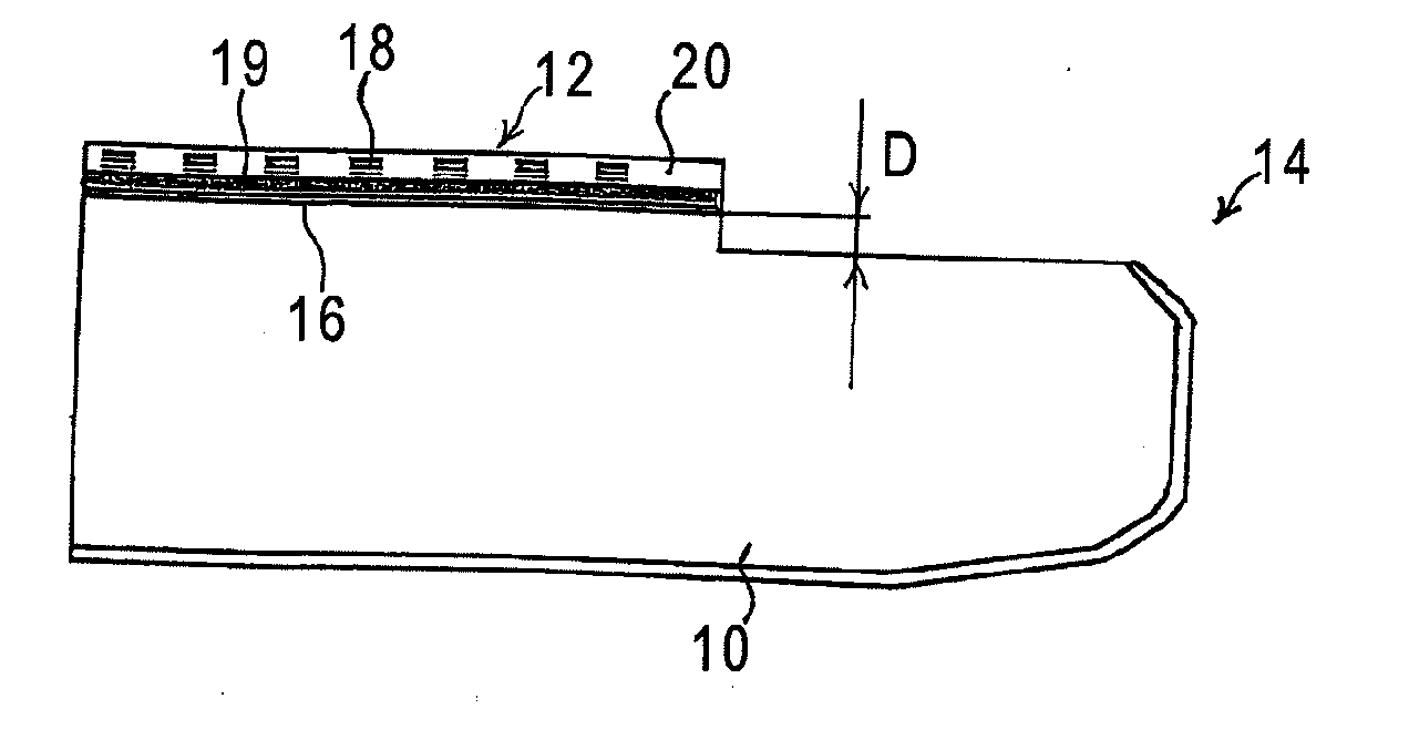
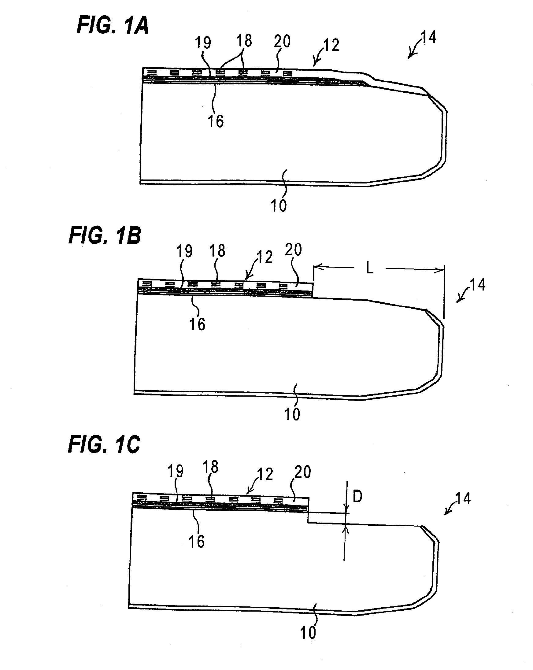
[0038]First, as shown in FIG. 1A, a device substrate (silicon substrate) 14, having a deposited film 12, such as an interconnect film, on a surface of silicon (bare silicon) 10, is prepared. In this embodiment, the deposited film (interconnect film) 12 consists of a silicon layer 16, an oxide film 20 that covers device interconnects 18 formed on the surface of the silicon layer 16, and a nitride film (SiN film) 19 formed between the silicon layer 16 and the oxide film 20.

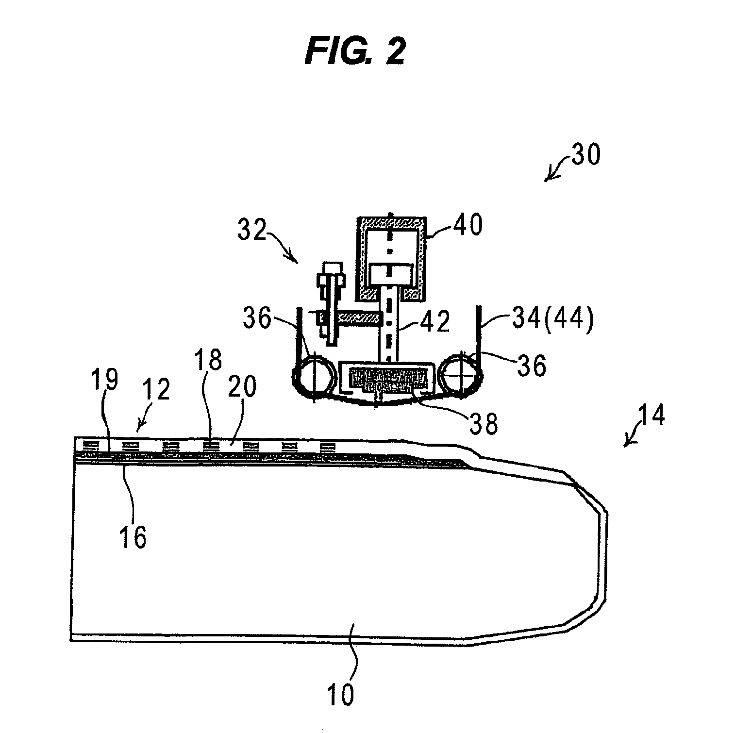
[0039]Next, as shown in FIG. 1B, the deposited film 12, lying in the width L peripheral portion of the device substrate 14, is removed to expose the silicon 10 in the peripheral portion of the device substrate 14. The width L is, for example, 0.3 to 80 mm. The removal of the deposited film 12 is carried out, e.g., by using a polishing apparatus 30 as shown in FIG. 2. The polishing apparatus 30 includes...


PUM

PropertyMeasurementUnit
Angular velocityaaaaaaaaaa
Thicknessaaaaaaaaaa

Abstract

A method for manufacturing a semiconductor device makes it possible to efficiently polish with a polishing tape a peripheral portion of a silicon substrate under polishing conditions particularly suited for a deposited film and for silicon underlying the deposited film. The method includes: pressing a first polishing tape against a peripheral portion of a device substrate having a deposited film on a silicon surface while rotating the device substrate at a first rotational speed, thereby removing the deposited film lying in the peripheral portion of the device substrate and exposing the underlying silicon; and pressing a second polishing tape against the exposed silicon lying in the peripheral portion of the device substrate while rotating the device substrate at a second rotational speed, thereby polishing the silicon to a predetermined depth.

Description

BACKGROUND OF THE INVENTION[0001]1. Field of the Invention[0002]The present invention relates to a method for manufacturing a semiconductor device, and more particularly to a method for use in the manufacturing of an SOI (silicon-on-insulator) substrate by a bonding method which involves bonding, through heat treatment or the like, two silicon substrates: a device substrate having semiconductor devices, and a supporting substrate.[0003]2. Description of the Related Art[0004]A bonding method, which involves bonding, through heat treatment or the like, two silicon substrates (a device substrate and a supporting substrate), is known as a method for manufacturing an SOI substrate. When manufacturing an SOI substrate by such a boding method, it is necessarily to remove a peripheral non-bonded portion of bonded two substrates from the SOI substrate.[0005]A method is known in which a first silicon substrate (device substrate), having a semiconductor layer (SIO layer) in a surface and whose...

Claims


Application Information

Patent Timeline
IPC IPC(8): H01L21/762
CPCB24B9/065B24B21/002B24B37/042H01L21/02038H01L21/304H01L21/76256H01L21/02087H01L21/7624
Inventor NAKANISHI, MASAYUKITOGAWA, TETSUJIITO, KENYASEKI, MASAYAIWADE, KENJIKUBOTA, TAKEO
Owner KIOXIA CORP
Why Eureka
Try Eureka