

Link processing with high speed beam deflection
- Summary
- Abstract
- Description
- Claims
- Application Information
AI Technical Summary
Benefits of technology
Problems solved by technology
Method used
Image

Examples
Embodiment Construction
Overview
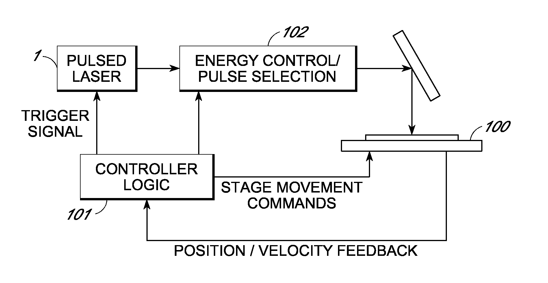
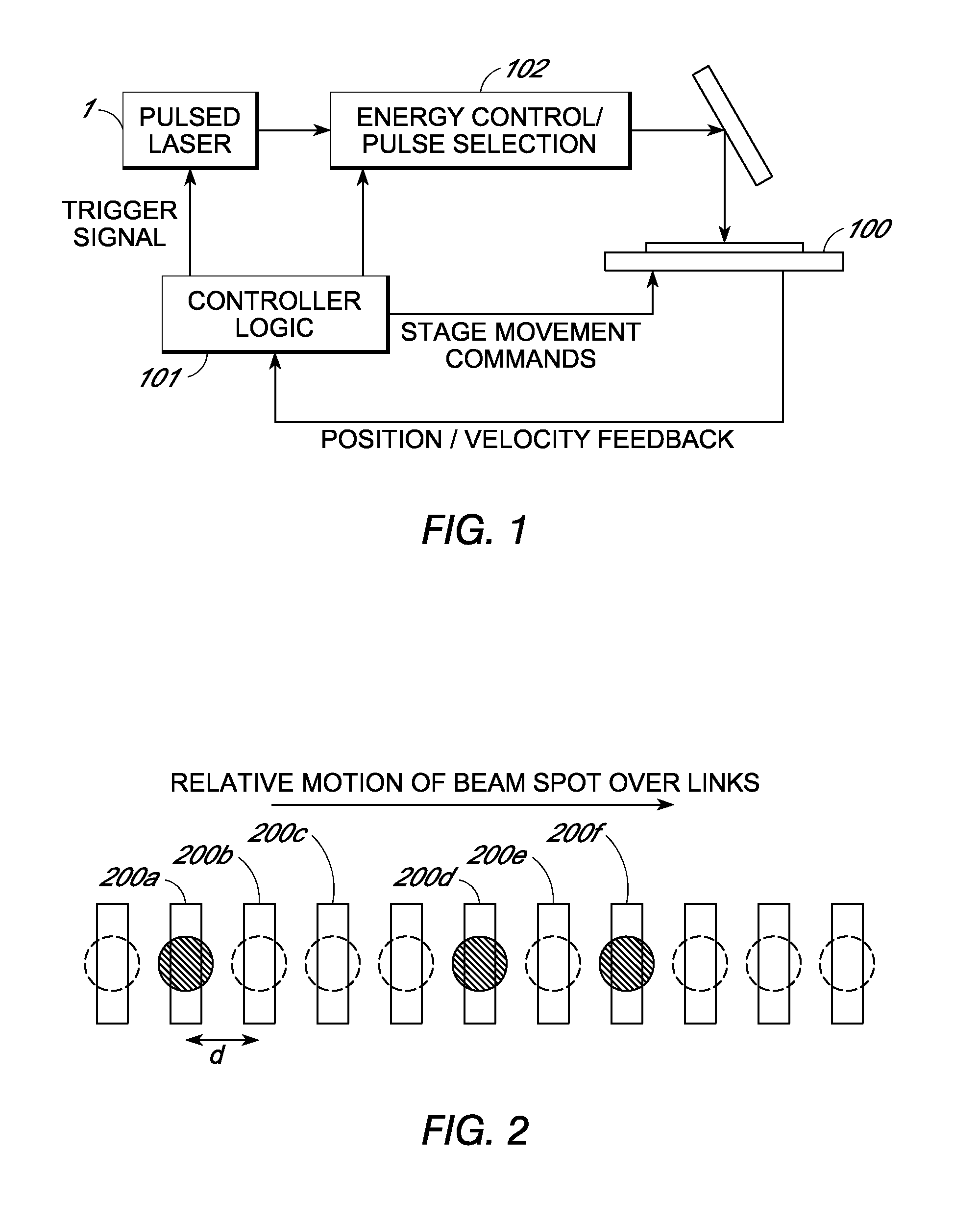
[0060]Multi-axis inertialess beam positioning is used to access processing targets relative to the trajectory of a mechanical positioning system to sever conductive links at high rates. Various laser processing aspects using split and / or deflected beams are disclosed in US patent publication 2009 / 0095722. This document is incorporated herein by reference and forms part of this application. The present disclosure is primarily directed to rapid access with a single beam. In particular, the approach uses high speed positioning within a two dimensional random access field that moves along a trajectory relative to the wafer. Positioning laser spots within the field at a processing rate allows flexible access to links passing through the field along the trajectory with a throughput exceeding a conventional link pitch based processing rate. Elapsed time traditionally required for passing over unprocessed links can be reduced, a higher percentage of laser pulses are used for process...
PUM
| Property | Measurement | Unit |
|---|---|---|
| Diameter | aaaaa | aaaaa |
| Time | aaaaa | aaaaa |
| Angle | aaaaa | aaaaa |
Abstract
Description
Claims
Application Information