Light emitting device, resin package, resin-molded body, and methods for manufacturing light emitting device, resin package and resin-molded body
- Summary
- Abstract
- Description
- Claims
- Application Information
AI Technical Summary
Benefits of technology
Problems solved by technology
Method used
Image
Examples
first embodiment
[0035](Light Emitting Device)
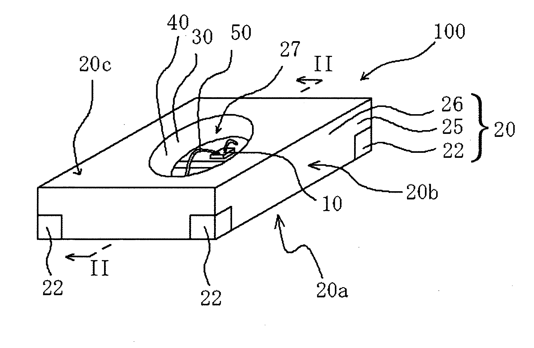
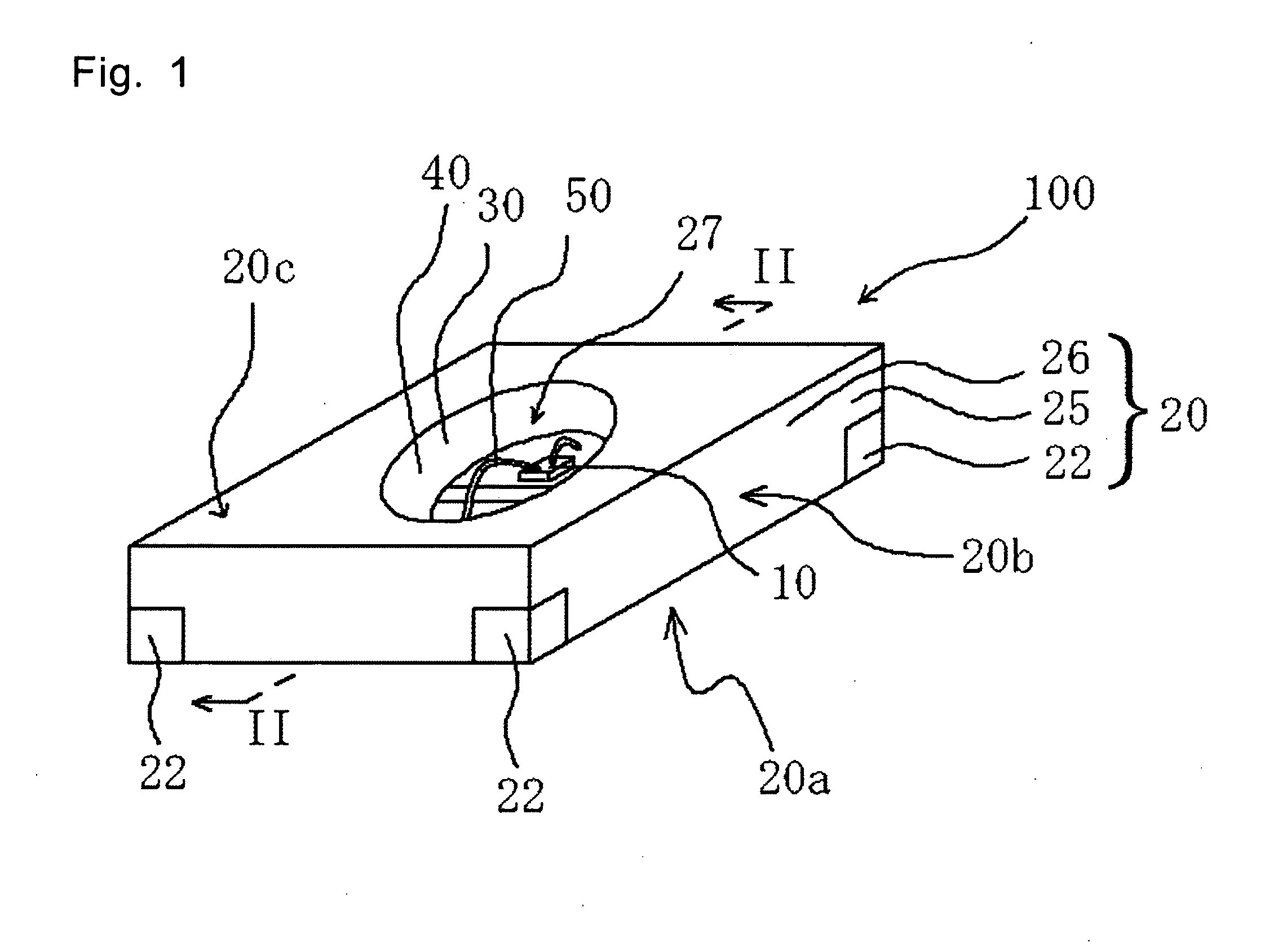
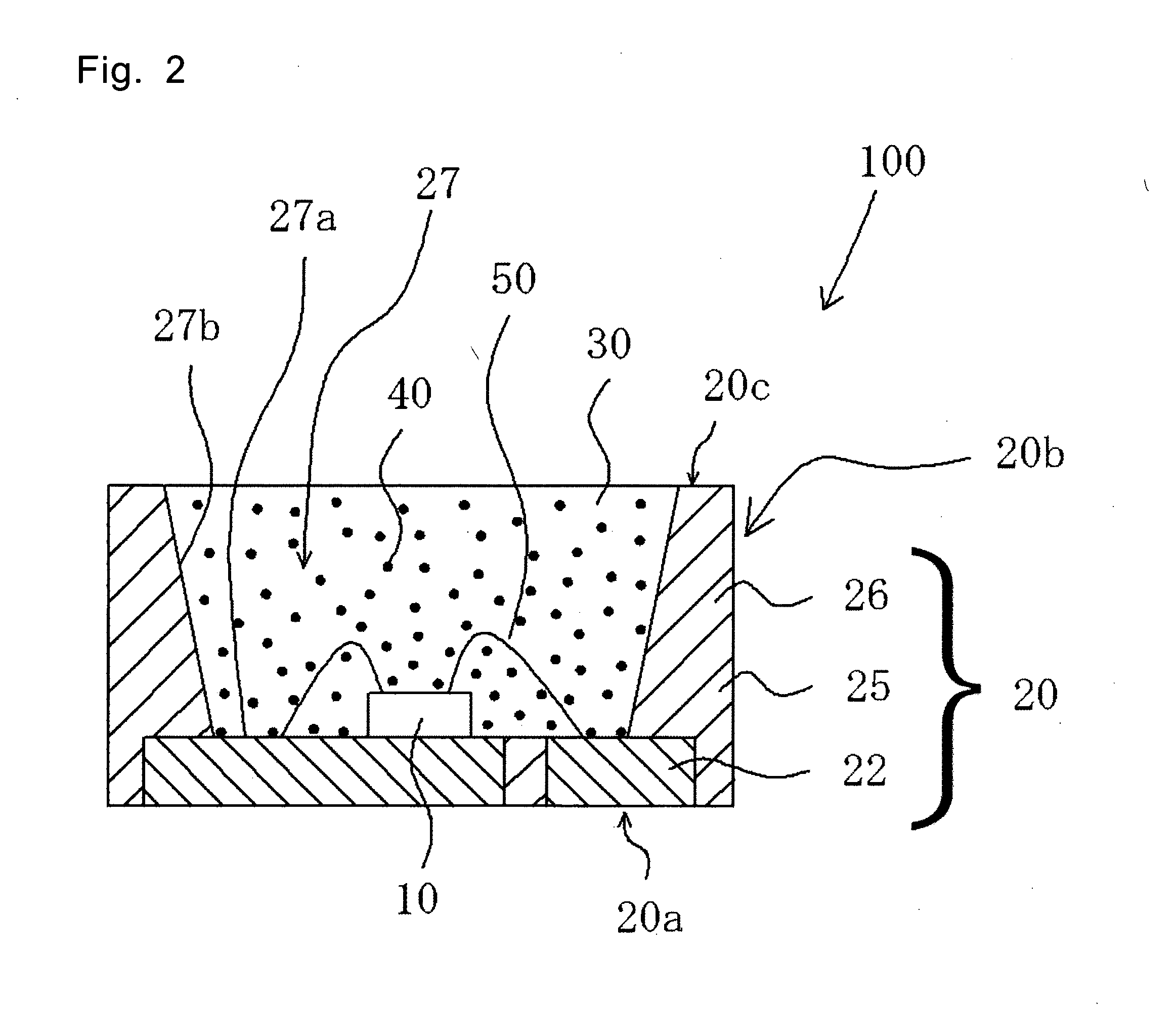
[0036]A light emitting device according to a first embodiment will be described. FIG. 1 is a perspective view illustrating a light emitting device according to the first embodiment. FIG. 2 is a sectional view illustrating a light emitting device according to the first embodiment. FIG. 2 is a sectional view taken along line II-II illustrated in FIG. 1. FIG. 3 is a plan view illustrating a lead frame used in the first embodiment.
[0037]A light emitting device 100 according to the first embodiment provides an optical reflectivity equal to or greater than 70% at the wavelength between 350 nm and 800 nm after thermal curing, and has a resin package 20 in which a resin part 25 and leads 22 are formed in the substantially same plane in outer side surfaces 20b. Plating processing is applied to at least one surface of the bottom surface (an outer bottom surface 20a of the resin package 20) and the upper surface (an inner bottom surface 27a of a concave part 27) of...
second embodiment
[0098]A light emitting device according to a second embodiment will be described. FIG. 6 is a perspective view illustrating a light emitting device according to the second embodiment. FIG. 7 is a plan view illustrating a lead frame used in the second embodiment. FIG. 8 is a plan view illustrating a resin-molded body according to the second embodiment. Description of some configurations employing the substantially same configuration as the light emitting device according to the first embodiment will be omitted where necessary.
[0099]With the light emitting device according to the second embodiment, the light emitting element 10 is placed in the concave part provided in the resin package 120. The corner parts of the outer upper surface 120c of the resin package 120 are formed in an arc shape. Further, the side surface of the lead 122 is formed in an arc shape seen from the upper surface, and the lead 122 is provided with a step such that the lead 122 slightly projects from the resin pa...
third embodiment
[0108]A light emitting device according to a third embodiment will be described. FIG. 9 is a perspective view illustrating the light emitting device according to the third embodiment. FIG. 10 is a plan view illustrating a lead frame used in the third embodiment. Description of some configurations employing the substantially same configuration as the light emitting device according to the first embodiment will be omitted where necessary.
[0109]The light emitting device according to the third embodiment provides an optical reflectivity equal to or greater than 70% at the wavelength between 350 nm and 800 nm after thermal curing, and has a resin package 220 in which a resin part 225 and leads 222 are formed in the substantially same plane in an outer side surface 220b. Plating processing is applied to the bottom surface and upper surface of the leads 222, and is not applied to the outer side surfaces. The lead 222 has a predetermined thickness, and is provided with differences in level ...
PUM
| Property | Measurement | Unit |
|---|---|---|
| Fraction | aaaaa | aaaaa |
| Nanoscale particle size | aaaaa | aaaaa |
| Nanoscale particle size | aaaaa | aaaaa |
Abstract
Description
Claims
Application Information


