Semiconductor device and microphone

a technology of semiconductor devices and microphones, applied in the direction of piezoelectric/electrostrictive transducers, electrostatic transducers of semiconductors, transducers, etc., can solve the problems of complex structure of the package or wiring structure, and achieve the effect of facilitating the wire bonding process, facilitating the assembly accuracy of semiconductor devices, and facilitating the image recognition of the bonding pad and the first joint portion

Active Publication Date: 2011-09-15
MMI SEMICON CO LTD
View PDF4 Cites 34 Cited by
  • Summary
  • Abstract
  • Description
  • Claims
  • Application Information

AI Technical Summary

Benefits of technology

[0024]In another embodiment of the semiconductor device according to one or more embodiments of the present invention, the bonding pad and the first joint portion are positioned in a same plane parallel to a bottom surface of the recess. According to such embodiment, the process of wire bonding is facilitated because the direction of wire bonding at the bonding pad and the direction of wire bonding with respect to the semiconductor element mounted on the bottom surface of the recess are the same direction. The assembly accuracy of the semiconductor device is also enhanced. For instance, the image recognition of the bonding pad and the first joint portion is facilitated.
[0025]In another embodiment of the semiconductor according to one or more embodiments of the present invention, the bonding pad and the first joint portion are positioned in different planes parallel to the bottom surface of the recess. According to such embodiment, the process of wire bonding is facilitated because the direction of wire bonding at the bonding pad and the direction of wire bonding with respect to the semiconductor element mounted on the bottom surface of the recess are the same direction. Further, the wire wiring is less likely to contact the second member because the bonding pad is slightly spaced apart from the second member.
[0026]In another embodiment of the semiconductor device according to one or more embodiments of the present invention, an outer peripheral edge of the first joint portion is higher than a region on the inner side. According to such embodiment, the conduction unit is less likely to leak outside from the first joint portion even if the conduction unit is a solder or a conductive adhesive.

Problems solved by technology

Therefore, in the microphone of the prior art in which the member (cover) mounted with the microphone chip and the member (substrate) including the signal input / output unit of the microphone are separate members, the structure of the package or the wiring structure is complicated because the bonding pad is arranged on the same surface as the surface mounted with the semiconductor device.

Method used


Image

  • Semiconductor device and microphone
  • Semiconductor device and microphone
  • Semiconductor device and microphone

Examples


first embodiment

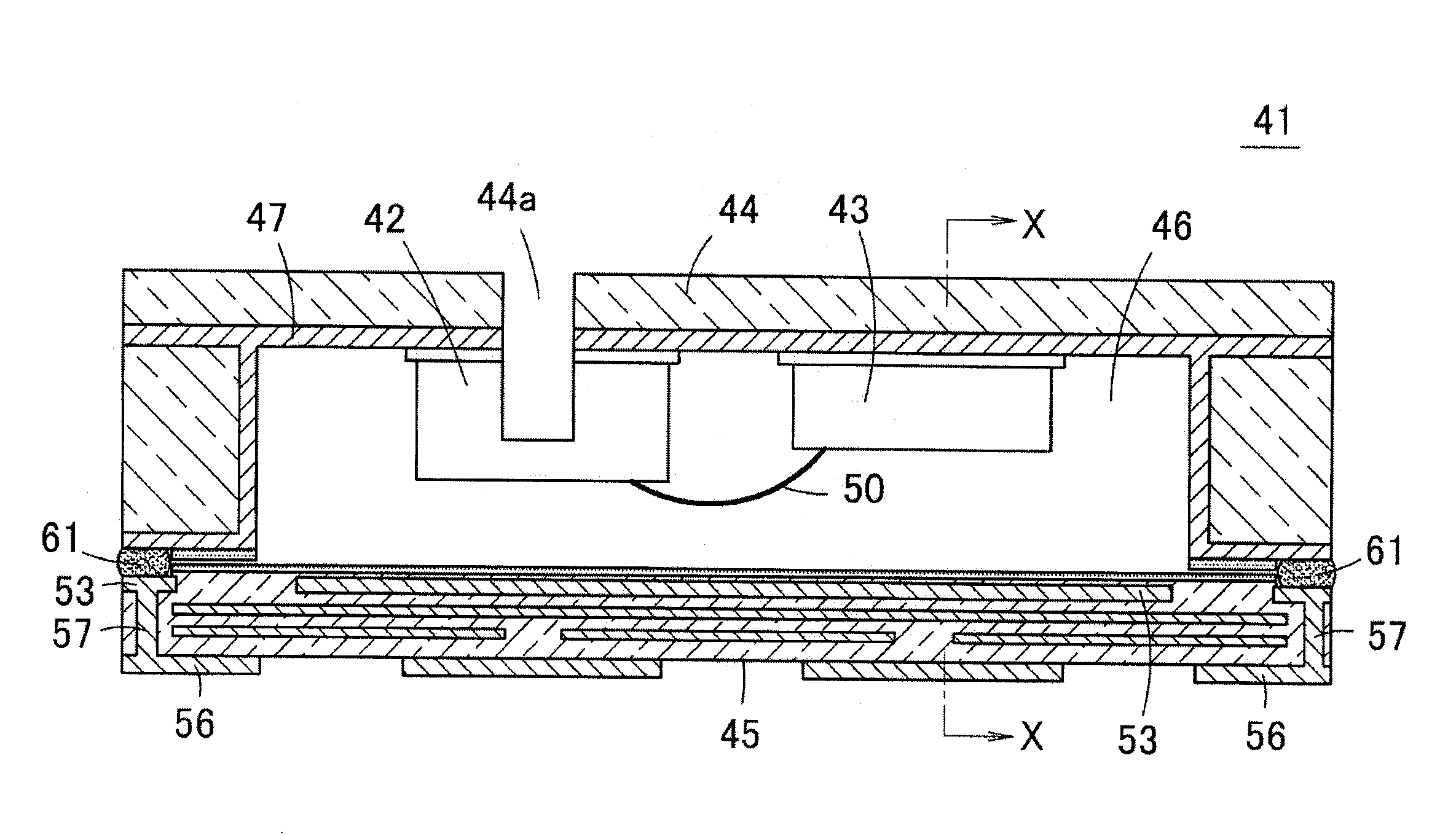
[0065]A top port type microphone 41 according to a first embodiment of the present invention will be described below with reference to FIG. 3, FIG. 4, and FIG. 5. FIG. 3 is a cross-sectional view showing a cross-section taken along a longitudinal direction of the microphone 41. FIG. 4 is a cross-sectional view showing a cross-section in a width direction taken along line X-X of FIG. 3. The microphone 41 is an MEMS microphone manufactured using the MEMS technique.

[0066]The microphone 41 has a microphone chip 42 and a circuit element 43 accommodated in a package including a cover 44 and a substrate 45. FIG. 5A is a bottom view of the cover 44 (first member) mounted with the microphone chip 42 and the circuit element 43, and FIG. 5B is a top view of the substrate 45 (second member). FIG. 5A also shows a state in which the solder resist of the elliptical portion is removed.

[0067]As shown in FIG. 3 and FIG. 4, the cover 44 is formed by laminating two insulating substrates including at le...

second embodiment

[0074]FIG. 6 is a cross-sectional view taken along the width direction of a microphone 71 according to a second embodiment of the present invention. The cross-section taken along the longitudinal direction of the microphone 71 is shown similarly to FIG. 3. FIG. 7A is a bottom view of the cover 44 mounted with the microphone chip 42 and the circuit element 43, and FIG. 7B is a top view of the substrate 45.

[0075]In the present embodiment, an electrode plate 72 insulated from the conductive layer 47 is arranged at the lower surface of the cover 44, and the central part of the electrode plate 72 is covered with the solder resist 52 to divide the electrode plate 72 into two regions. One of the regions of the electrode plate 72 divided by the solder resist 52 is the bonding pad 48 for bonding the end of the bonding wire 51a, and the other region of the electrode plate 72 is a joining pad 73 (first joint portion) for joining the connection electrode 54 (second joint portion) with the condu...

third embodiment

[0077]FIG. 8 is a cross-sectional view taken along the longitudinal direction of a microphone 81 according to a third embodiment of the present invention, and FIG. 9 is a cross-sectional view taken along the width direction of the microphone 81. FIG. 10A is a bottom view of the cover 44 mounted with the microphone chip 42 and the circuit element 43, and FIG. 10B is a top view of the substrate 45.

[0078]In the microphone 81, a peripheral wall 82 is raised at the periphery of the upper surface of the substrate 45, and a depression 83 surrounded with the peripheral wall 82 is formed on the upper surface of the substrate 45. The cover 44 is overlapped on the substrate 45 such that the lower surface is mounted on the upper surface of the peripheral wall 82, and the outer peripheral part of the conductive layer 47 is joined to the conductive layer 53 positioned at the outer peripheral part of the upper surface of the peripheral wall 82 by the conductive member 61. Furthermore, the connecti...


PUM


Abstract

The semiconductor device has a simplified structure which includes a package structure in which a member for mounting a semiconductor element is separate from a member including a signal input/output unit. A microphone package is configured with a cover and a substrate. A microphone chip and a circuit element are adhered and fixed to a top surface of a recess formed in the cover. A plurality of bonding pads are arranged on the lower surface of the cover on the outer side of the recess. A bonding wire is connected to the circuit element and the bonding pad. The substrate includes a signal input/output terminal serving as the signal input/output unit, and a connection electrode, conducted with the signal input/output terminal, is arranged facing the bonding pad on the upper surface of the substrate. The substrate, cover, connection electrode, and bonding pad are joined with a conductive member.

Description

BACKGROUND OF THE INVENTION[0001]1. Technical Field[0002]One or more embodiments of the present invention relates to semiconductor devices and microphones. Specifically, one or more embodiments of the present invention relate to a semiconductor device in which a semiconductor element is accommodated in a package. One or more embodiments of the present invention also relates to a microphone in which a microphone chip (acoustic sensor) is accommodated in a package.[0003]2. Related Art[0004]A microphone manufactured using the MEMS (Micro Electro-Mechanical Systems) technique generally has a structure in which an MEMS microphone chip is accommodated in a package configured by a substrate and a cover. The microphone includes that in which the microphone chip is mounted on the cover and that in which the microphone chip is mounted on the substrate. An acoustic hole for introducing the acoustic vibration into the package may be opened in the cover or may be opened in the substrate.[0005]Th...

Claims


Application Information

Patent Timeline
Patent Type & Authority Applications(United States)
IPC IPC(8): H04R11/04H01L29/84
CPCH04R19/005H04R19/04H04R31/00H01L2224/48091H01L2924/3025H01L2224/49171H01L2224/73265H01L2924/1461H01L2224/48137H01L2924/00014H01L2924/00H01L23/48
Inventor KURATANI, NAOTOONO, KAZUYUKIMAEKAWA, TOMOFUMI
Owner MMI SEMICON CO LTD
Why Eureka
Try Eureka