Method of manufacturing a multilayer printed circuit board with a built-in electronic device

a printed circuit board and electronic device technology, applied in the direction of printed circuit aspects, printed circuit components, conductive pattern formation, etc., can solve the problems of reducing reliability, multi-functionality, and the greatest limitation of the area occupied by the electronic device for miniaturizing the product, so as to reduce the volume and weight of the printed circuit board, enhance the function, and increase the pressure resistance

Active Publication Date: 2011-09-22
UNITECH PRINTED CIRCUIT BOARD CORP
View PDF7 Cites 18 Cited by
  • Summary
  • Abstract
  • Description
  • Claims
  • Application Information

AI Technical Summary

Benefits of technology

[0009]Therefore, it is a primary objective of the invention to overcome the shortcomings of the prior art by providing a method of manufacturing a multilayer printed circuit board with a built-in electronic device, and the method can accommodate more electronic devices in the limited space of a copper clad laminate to achieve the effects of enhancing the function and reducing the volume and weight of the printed circuit board, wherein the built-in electronic device is an active component, a passive component or a light emitting element.
[0010]Another objective of the present invention is to increase the pressure resistance by a dielectric layer during a later build-up process of circuits, so as to prevent the embedded electronic devices from being damaged by pressing during the manufacturing process.

Problems solved by technology

Thus, electronic and mobile communication products tend to be developed with a light, thin, short and compact design and come with multi-functions, high reliability and low price.
As to a printed circuit board, the area occupied by the electronic devices has been the greatest limitation for miniaturizing the products.
With too many soldering points on the printed circuit board, the reliability will be lowered, and the manufacturing cost will be increased.
However, when the conductive foil coupled with the passive component is laminated onto the organic insulating layer, the passive component has a specific height, and there is a risk of damaging the components or affecting the product reliability, since the organic insulating layer will press the components directly during a thermal pressing process.

Method used


Image

  • Method of manufacturing a multilayer printed circuit board with a built-in electronic device
  • Method of manufacturing a multilayer printed circuit board with a built-in electronic device
  • Method of manufacturing a multilayer printed circuit board with a built-in electronic device

Examples


Embodiment Construction

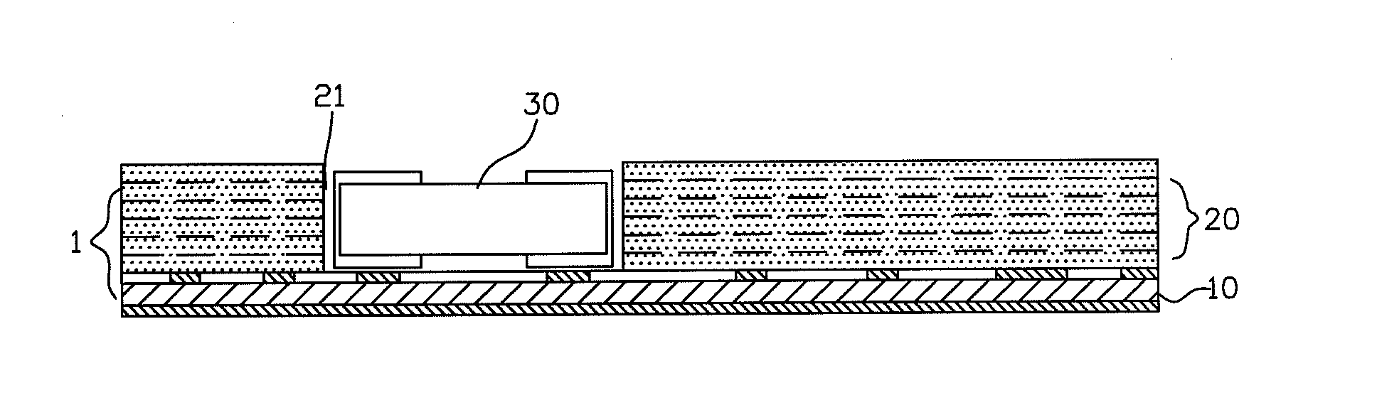
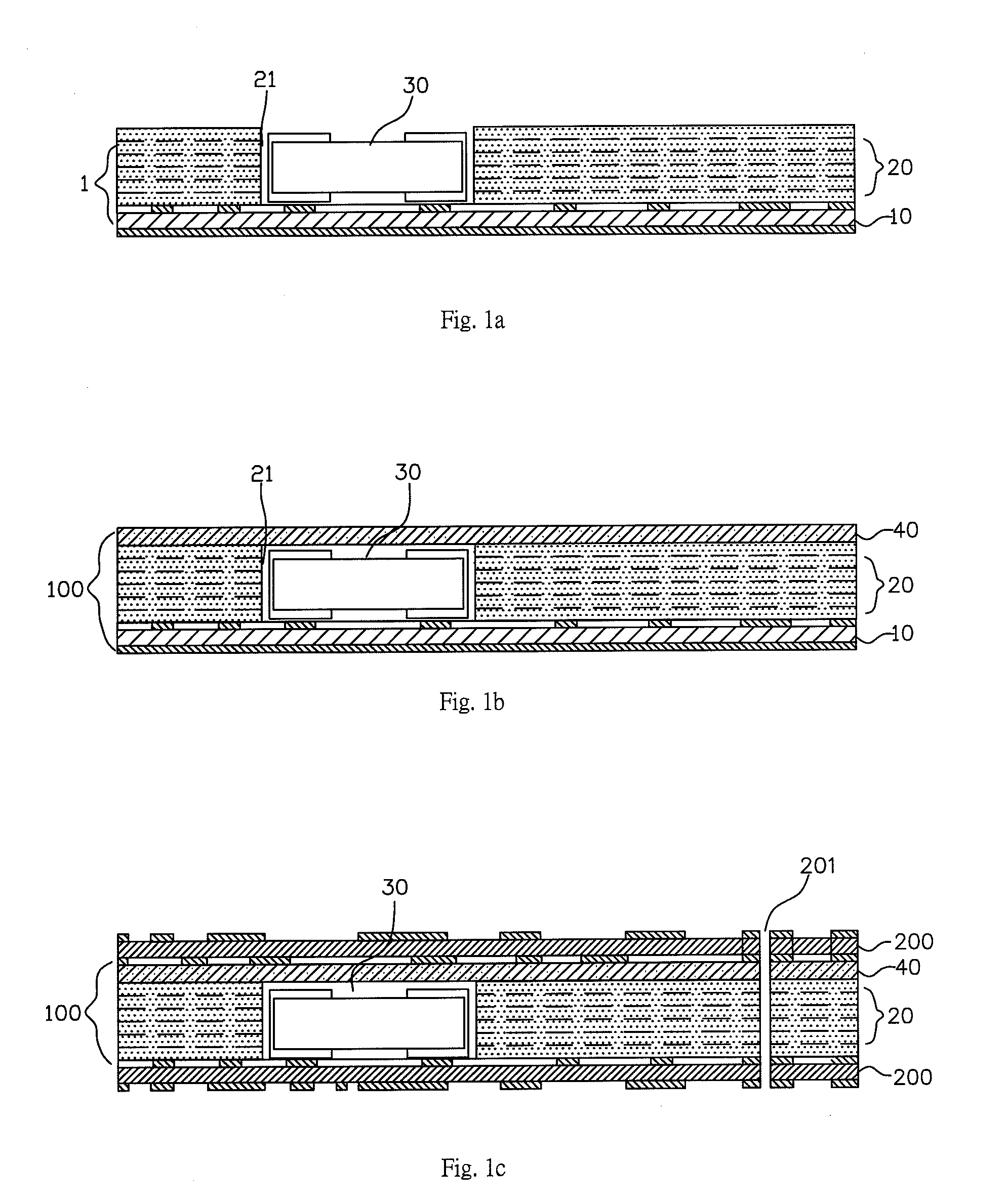
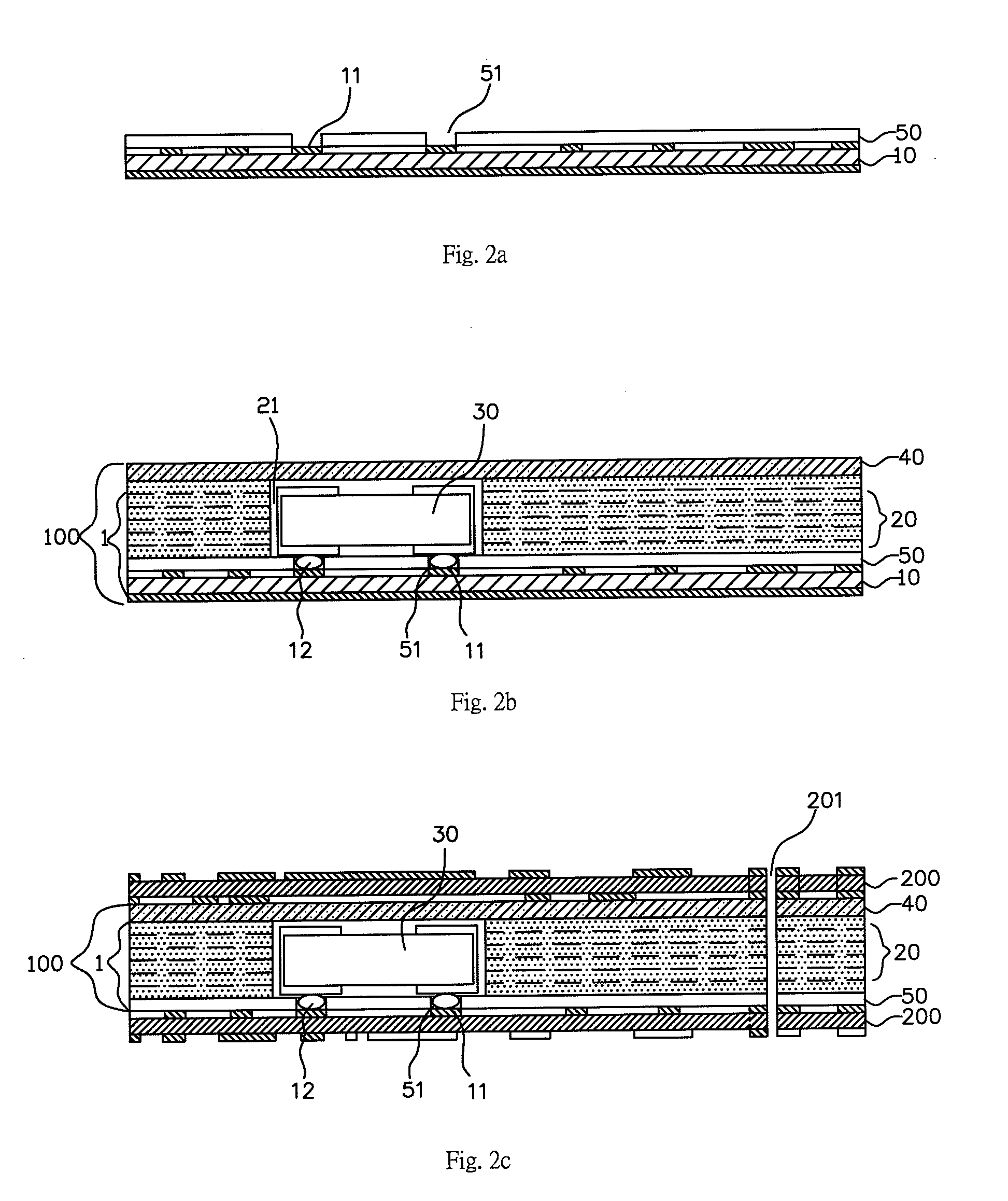
[0022]With reference to FIGS. 1a˜1c for a method of manufacturing a multilayer printed circuit board of a built-in electronic device in accordance with the present invention, the manufacturing method comprises the steps of:

[0023]providing a substrate 1 as shown in FIG. 1a, wherein the substrate 1 includes a copper clad laminate 10 and a first dielectric layer 20;

[0024]installing an electronic device 30 on the copper clad laminate 10;

[0025]laminating the first dielectric layer 20 onto the copper clad laminate 10, and performing a cavity 21 at a position capable of accommodating the electronic device 30 precisely, wherein the first dielectric layer of this preferred embodiment is a sheet body (and the first dielectric layer can be made of laminating single-layer or multilayer sheets);

[0026]laminating a second dielectric layer 40 onto the substrate 1 as shown in FIG. 1b, wherein the second dielectric layer of this preferred embodiment is a sheet body (and the second dielectric layer ca...


PUM

PropertyMeasurementUnit
plastic propertyaaaaaaaaaa
dielectricaaaaaaaaaa
electricallyaaaaaaaaaa

Abstract

A method of manufacturing a multilayer printed circuit board of a built-in electronic device provides a substrate having a copper clad laminate and a first dielectric layer. The first dielectric layer is laminated onto the copper clad laminate and has a cavity for accommodating the electronic device. A second dielectric layer is laminated onto the substrate and electronic device to produce a base circuit board with an embedded electronic device. A build-up circuit layer is formed on the base circuit board. The first and second dielectric layers are made of a plastic material.

Description

BACKGROUND OF THE INVENTION[0001]1. Field of the Invention[0002]The present invention relates to a method of manufacturing a multilayer printed circuit board, and more particularly to a method of manufacturing a multilayer printed circuit board with a built-in electronic device.[0003]2. Description of the Related Art[0004]At present, speed and density are two major requirements of the development of high technologies, and it is a primary objective to satisfy consumer requirements as well as lowering the production cost. Thus, electronic and mobile communication products tend to be developed with a light, thin, short and compact design and come with multi-functions, high reliability and low price. These products are generally developed in generations of every three to five years. To comply with this trend, passive components occupying the largest area in a circuit design of electronic products are integrated.[0005]As to a printed circuit board, the area occupied by the electronic dev...

Claims


Application Information

Patent Timeline
Patent Type & Authority Applications(United States)
IPC IPC(8): H05K3/00
CPCH05K1/185H05K1/186H05K1/188H05K3/3442H05K2201/09063H05K2201/10106Y10T29/49165H05K2203/1469H05K2203/167Y10T29/49124Y10T29/49126Y10T29/49155H05K2203/063H01L2224/04105H01L2224/2518H01L2224/92144
Inventor CHOU, CHENG-HSIENHSU, SHUN-YUEHCHEN, KUN-CHICHEN, HUNG-MIN
Owner UNITECH PRINTED CIRCUIT BOARD CORP
Why Eureka
Try Eureka