Light emitting diode chip and method for manufacturing the same

a technology of light-emitting diodes and manufacturing methods, which is applied in the direction of semiconductor/solid-state device manufacturing, electrical apparatus, semiconductor devices, etc., can solve the problem that led also produces a large amount of hea

Inactive Publication Date: 2011-09-29
ADVANCED OPTOELECTRONICS TECH
View PDF2 Cites 12 Cited by
  • Summary
  • Abstract
  • Description
  • Claims
  • Application Information

AI Technical Summary

Problems solved by technology

However, the LED also pr...

Method used


Image

  • Light emitting diode chip and method for manufacturing the same
  • Light emitting diode chip and method for manufacturing the same
  • Light emitting diode chip and method for manufacturing the same

Examples


second embodiment

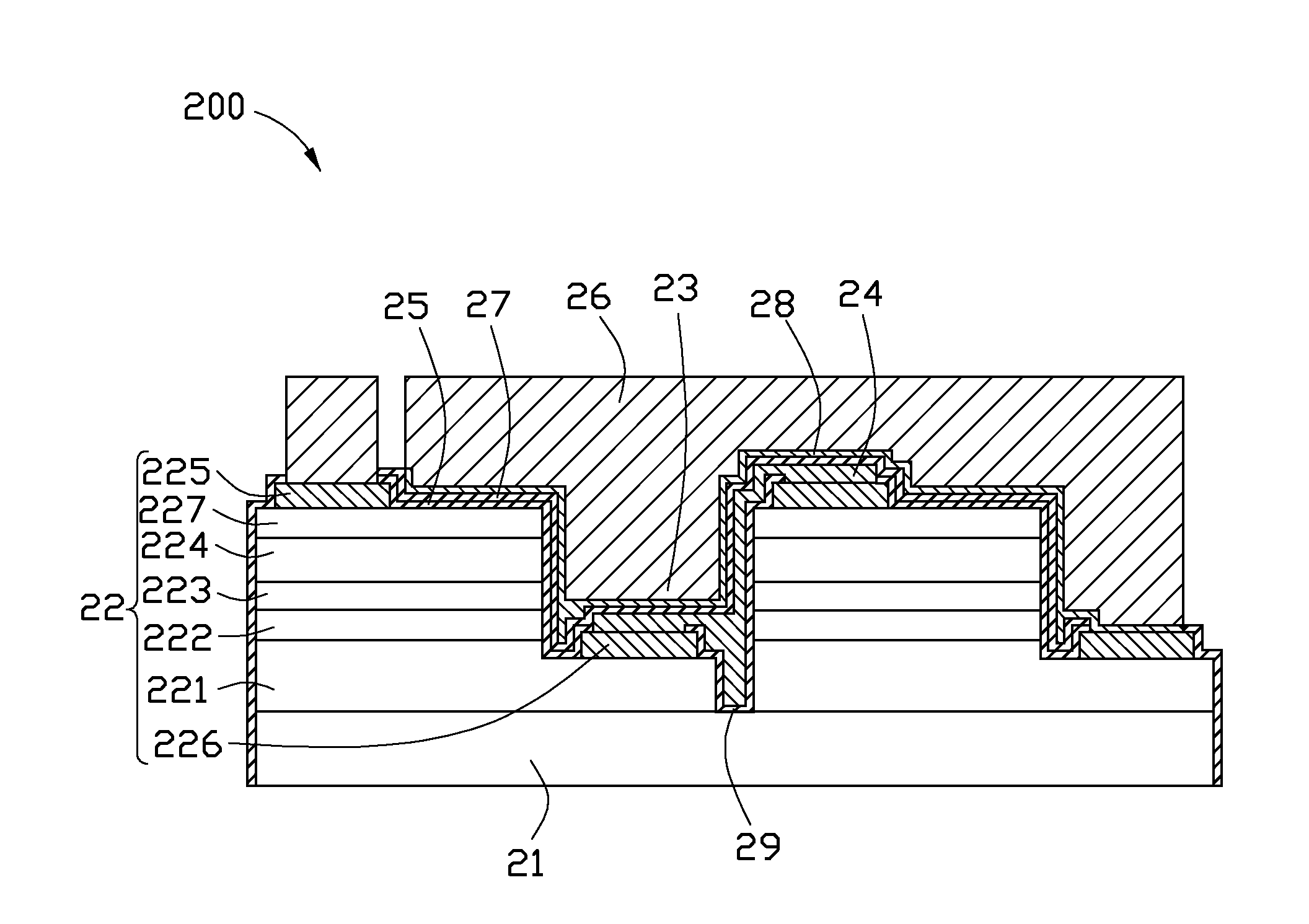
[0025]FIG. 3 shows a structure of an LED chip 200 in accordance with a The LED chip 200 includes a transparent substrate 21 and two lighting structure units 22. Each lighting structure unit 22 includes an n-type GaN layer 221, a first multiple quantum well active layer 222, a second multiple quantum well active layer 223, a p-type GaN layer 224, a p-type contacting electrode 225 and an n-type contacting electrode 226 deposited respectively on the p-type GaN layer 224 and the n-type GaN layer 221.

[0026]The lighting structure unit 22 has a recess 23. The recess 23 is defined extending from the p-type GaN layer 224 to the n-type GaN layer 221 and exposes the surface of the n-type GaN layer 221 for manufacturing the n-type contacting electrode 226 thereon.

[0027]The lighting structure unit 22 further includes a first electrical insulation layer 25. The first electrical insulation layer 25 totally covers the outside region of the p-type contacting electrode 225 and the n-type contacting ...

third embodiment

[0031]According to needs, the LED chip is not limited to two lighting structure units and can be three or more. FIG. 4 shows an electrical connection relationship of an LED chip 300 in accordance with a The LED chip 300 includes a transparent substrate 31 are four lighting structure units 32 arranged at the four corners of the transparent substrate 31. An isolating trench 39 is arranged between the lighting structure units 32.

[0032]Each lighting structure unit 32 includes a p-type contacting electrode 325 and an n-type contacting electrode 326. The lighting structure units 32 are electrically connected together in series by an electrical conducting metal layer 34.

[0033]A recess (not shown) is arranged at the lighting structure unit 32. A metal material 36 is filled inside the recess and the isolating trench 39 and covers the surface of the lighting structure units 32. Thus, the metal material 36 forms a larger heat dissipating surface.

[0034]In this embodiment, the metal material 36...


PUM


Abstract

An LED chip includes a transparent substrate and a number of lighting structure units each including a p-type semiconductor and an n-type semiconductor and a recess extending from the p-type semiconductor to the n-type semiconductor. The recess is filled with metal material which covers the surface of the lighting structure units. By filling the recess with metal material, the heat generated by the lighting structure units can rapidly transfer to the metal material. A method for manufacturing the light emitting diode chip is also provided.

Description

TECHNICAL FIELD[0001]The disclosure relates to light emitting diode chips, and particularly to a light emitting diode chip having high heat dissipating efficiency.DESCRIPTION OF THE RELATED ART[0002]Light emitting diodes (LEDs) have many advantages, such as high luminosity, low operational voltage, low power consumption, compatibility with integrated circuits, easy driving, long term reliability, and environmental friendliness, which have promoted their wide use as a light source. Now, light emitting diodes are commonly applied in environmental lighting.[0003]An LED includes a p-type semiconductor, an active layer, and an n-type semiconductor. When applying a voltage to the LED, the LED emits light. However, the LED also produces a larger amount of heat. Thus, the LED must overcome thermal dissipation challenges.[0004]Therefore, it is desirable to provide an LED which can overcome the described limitations.BRIEF DESCRIPTION OF THE DRAWINGS[0005]Many aspects of the disclosure can be ...

Claims


Application Information

Patent Timeline
IPC IPC(8): H01L33/00
CPCH01L27/153H01L2224/24H01L33/647H01L33/62
Inventor SHEN, CHIA-HUIHUNG, TZU-CHIEN
Owner ADVANCED OPTOELECTRONICS TECH
Why Eureka
Try Eureka