
Connection system for electronic components

a technology of electronic components and connection systems, applied in the direction of final product manufacturing, sustainable manufacturing/processing, semiconductor/solid-state device details, etc., can solve the problems of critical heat management of embedded components, embedded components that offer very poor heat transfer properties,

Active Publication Date: 2017-03-30
AT & S AUSTRIA TECH & SYSTTECHN AG
View PDF6 Cites 7 Cited by
  • Summary
  • Abstract
  • Description
  • Claims
  • Application Information

AI Technical Summary

Benefits of technology

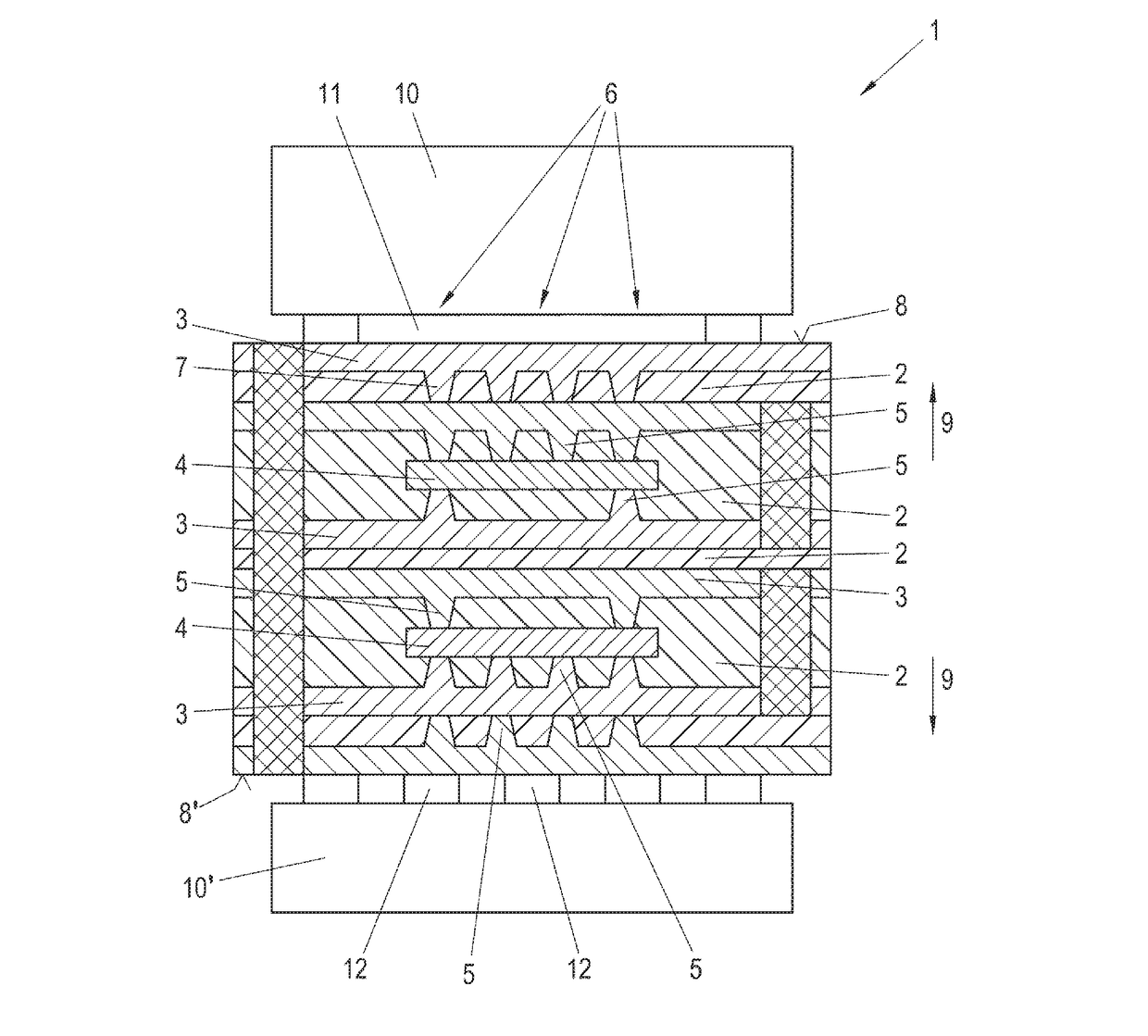
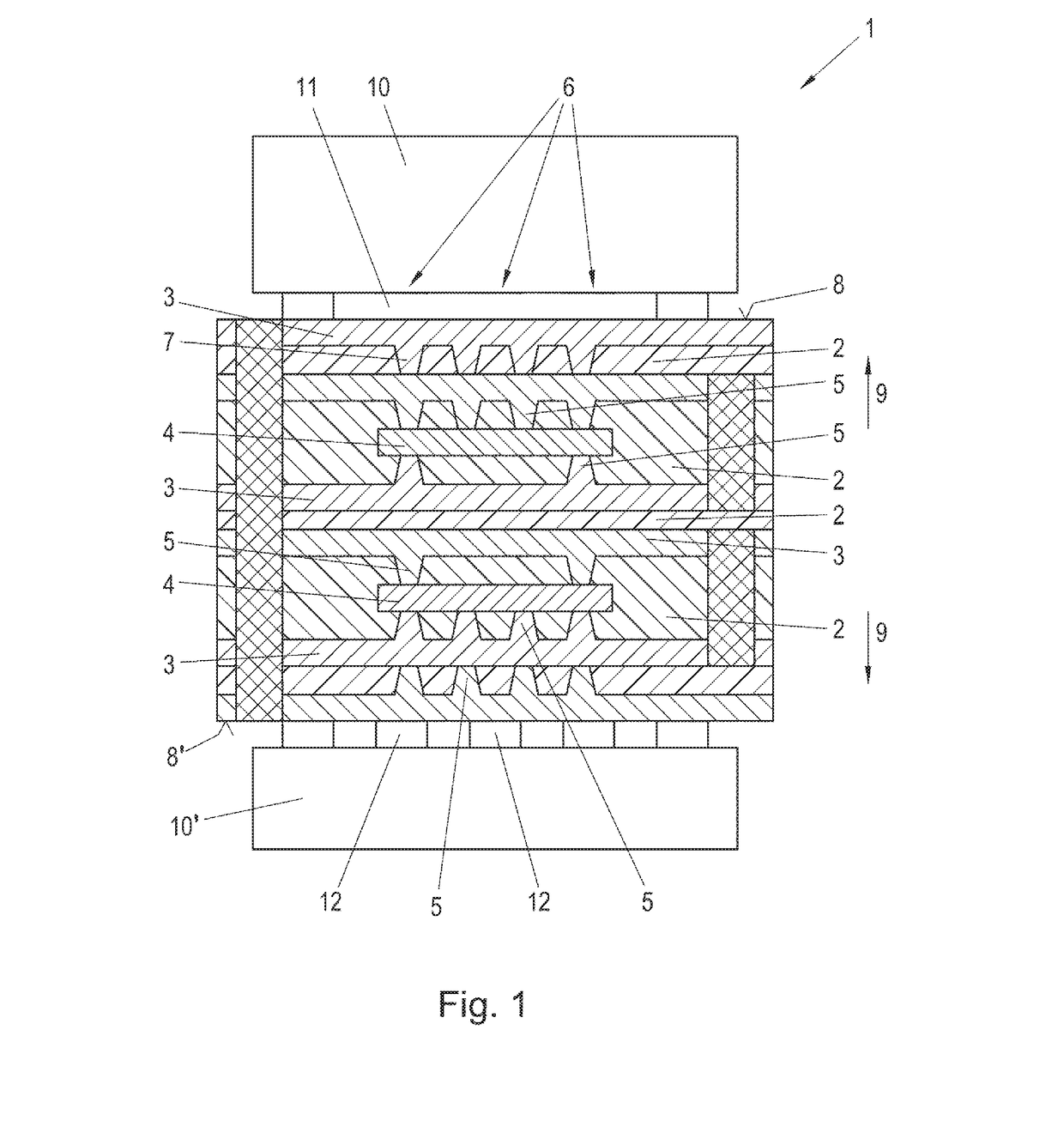
The invention is a connection system for electronic components that has a layered structure with at least one transistor and a second transistor arranged opposite each other. The system also includes vias that connect to surface-mounted electronic components on both sides of the connection system. The arrangement of the transistors helps to dissipate heat energy and avoid heat maxima that could damage the components. The system also includes a heat spreading plate and a conductive adhesive to improve heat transfer and secure the surface-mounted components. The use of anti-ferroelectric capacitors as surface-mounted components further enhances thermal management and efficiency. Overall, the invention provides improved heat dissipation and management for electronic components in a connection system.

Problems solved by technology

In the technical field of printed wiring boards, IC-substrates are known to offer similar functionality in terms of alternately applied conductive and insulating layers, however, IC-substrates are much smaller and often serve to connect a microchip to a printed circuit board.
Where there is a number of advantages related to embedded components in connection panels for electronic components, heat management of the embedded components is obviously a critical issue, especially when using high performance and / or high power components which produce considerable amounts of heat depending on the calculating load or on the currents that these components have to handle.
Insulating layers in which the embedded components are embedded offer very poor heat transfer properties so that special measures must be taken when considerable amounts of heat have to be dealt with at the location of the embedded components.

Method used


Image

  • Connection system for electronic components
  • Connection system for electronic components

Examples


Embodiment Construction

[0008]To achieve this object in accordance with the present invention, a connection system for electronic components of the initially mentioned kind is characterized in that the at least one embedded electronic component is at least one first transistor having a bulk terminal thereof in thermal contact with a thermal duct comprised of a plurality of vias reaching through at least one of an insulating layer and a conductive layer of the connection system for electronic components and emerging on a first outer surface of the connection system for electronic components under a first surface-mounted component. The invention is thus characterized by a thermal duct formed by a plurality of vias, which vias are adapted to guide heat from the embedded component not only to the surface thereof, but to a surface-mounted electronic component so that the heat guided away from the embedded component by the thermal duct is not only distributed on the surface of the connection system for electroni...


PUM


Abstract

In a connection system for electronic components (1) comprising a plurality of insulating layers (2) and conductive layers (3) and further comprising at least one embedded electronic component (4) embedded within at least one of the plurality of insulating layers (2) and conductive layers (3) the at least one embedded electronic component (4) is at least one first transistor having a bulk terminal thereof in thermal contact with a thermal duct (6) comprised of a plurality of vias (7) reaching through at least one of an insulating layer (2) and a conductive layer (3) of the connection system for electronic components (1) and emerging on a first outer surface (8) of the connection system for electronic components (1) under a first surface-mounted component (10).

Description

[0001]The invention relates to a connection system for electronic components comprising a plurality of insulating layers and conductive layers and further comprising at least one embedded electronic component embedded within at least one of the plurality of insulating layers and conductive layers.DESCRIPTION OF THE RELATED ART[0002]The invention relates to connection panels for electronic components in general, wherein electronic components such as transistors, integrated circuits (ICs, microchips) and the like are arranged on or embedded within a panel carrying and electrically connecting those electronic components. Such connection panels can be printed circuit boards (PCBs) or IC-substrates used for connecting a single integrated circuit or a plurality of integrated circuits to a printed circuit board. In fact, IC-substrates and printed circuit boards are highly similar in their basic functionalities and differ merely in size as will be explained and defined at a later stage of t...

Claims


Application Information

Patent Timeline
Patent Type & Authority Applications(United States)
IPC IPC(8): H01L25/16H05K1/02H05K1/11H05K7/20H01L23/467H01L25/07H01L23/00H05K1/18H01L23/538
CPCH01L25/16H01L2224/16227H05K1/185H05K1/0206H05K1/115H01L23/5389H01L23/5384H01L23/5383H01L23/467H01L25/074H01L24/17H05K7/20154H05K1/0298H05K2201/10166H01L2924/19041H01L2924/19102H05K2201/10015H01L2924/13055H01L2924/1306H01L2924/1033H01L2924/1426H05K1/181H05K1/0209H05K1/0212H01L23/3677H01L24/19H01L24/20H01L25/105H01L2223/6677H01L2224/04105H01L2224/12105H01L2224/2518H01L2225/1035H01L2225/1094H01L2924/1436H01L2924/19042H01L2924/19043H01L2924/19105H01L2924/153H01L2225/1047Y02P70/50
Inventor WEIS, GERALDVOCKENBERGER, CHRISTIANSEKAVCNIK, ROLAND
Owner AT & S AUSTRIA TECH & SYSTTECHN AG
Learn More