Lateral-diffusion metal-oxide semiconductor device and method for fabricating the same

a metal-oxide semiconductor and lateral-diffusion technology, applied in the direction of semiconductor devices, basic electric elements, electrical equipment, etc., can solve the problem of limiting the lateral-diffusion metal-oxide semiconductor device to obtain a satisfactory breakdown voltage, and achieve the effect of higher breakdown voltag

Active Publication Date: 2011-09-29
UNITED MICROELECTRONICS CORP
View PDF6 Cites 16 Cited by
  • Summary
  • Abstract
  • Description
  • Claims
  • Application Information

AI Technical Summary

Benefits of technology

[0008]It is an objective of the present invention to provide a LDMOS and method for fabricating the same to resolve the aforementioned issue of unable to achieve higher breakdown voltage.
[0009]According to a preferred embodiment of the present invention, a lateral-diffusion metal-oxide semiconductor (LDMOS) device is disclosed. The LDMOS device includes: a semiconductor substrate; at least one gate structure disposed on surface of the semiconductor substrate; a first well having a first conductive type, disposed in the semiconductor substrate adjacent to one side of the gate structure; a first isolation structure disposed in an upper portion of the first well and under a portion of the gate structure; a drain region disposed in the first well; a second isolation structure disposed in the semiconductor substrate adjacent to another side of the gate structure; a second well having a second conductive type, disposed in the semiconductor substrate between the second isolation structure and the gate structure; a source region disposed in the second well; and a deep well having the second c

Problems solved by technology

However, the doping concentration of the deep n-well fabricated by conventional method is typically uniform, hence the concentration difference at th

Method used


Image

  • Lateral-diffusion metal-oxide semiconductor device and method for fabricating the same
  • Lateral-diffusion metal-oxide semiconductor device and method for fabricating the same
  • Lateral-diffusion metal-oxide semiconductor device and method for fabricating the same

Examples


Embodiment Construction

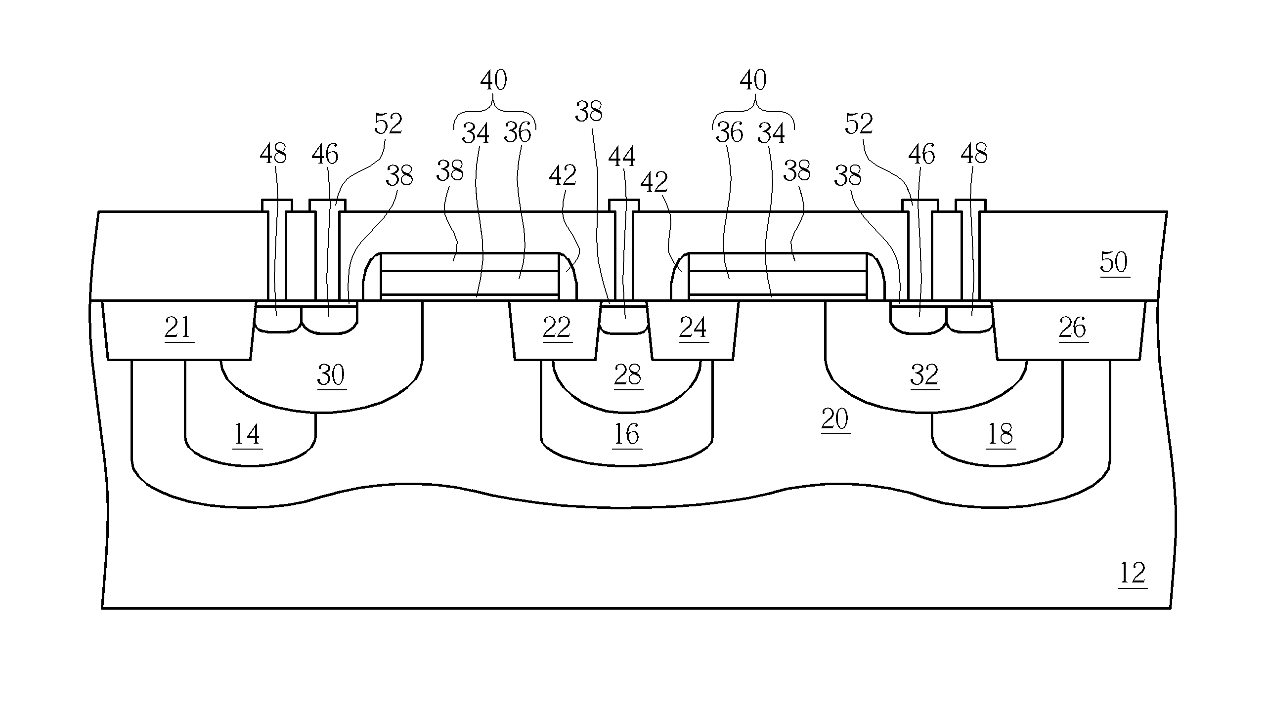
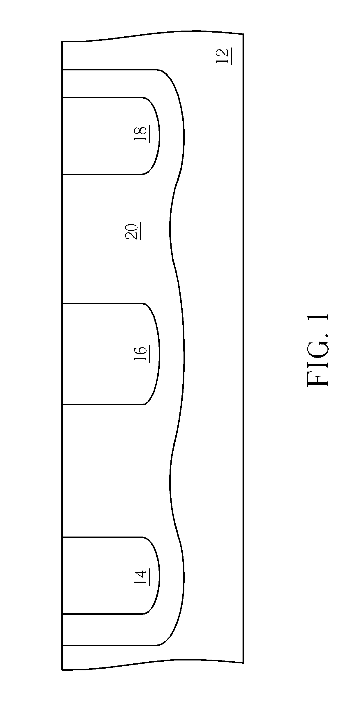
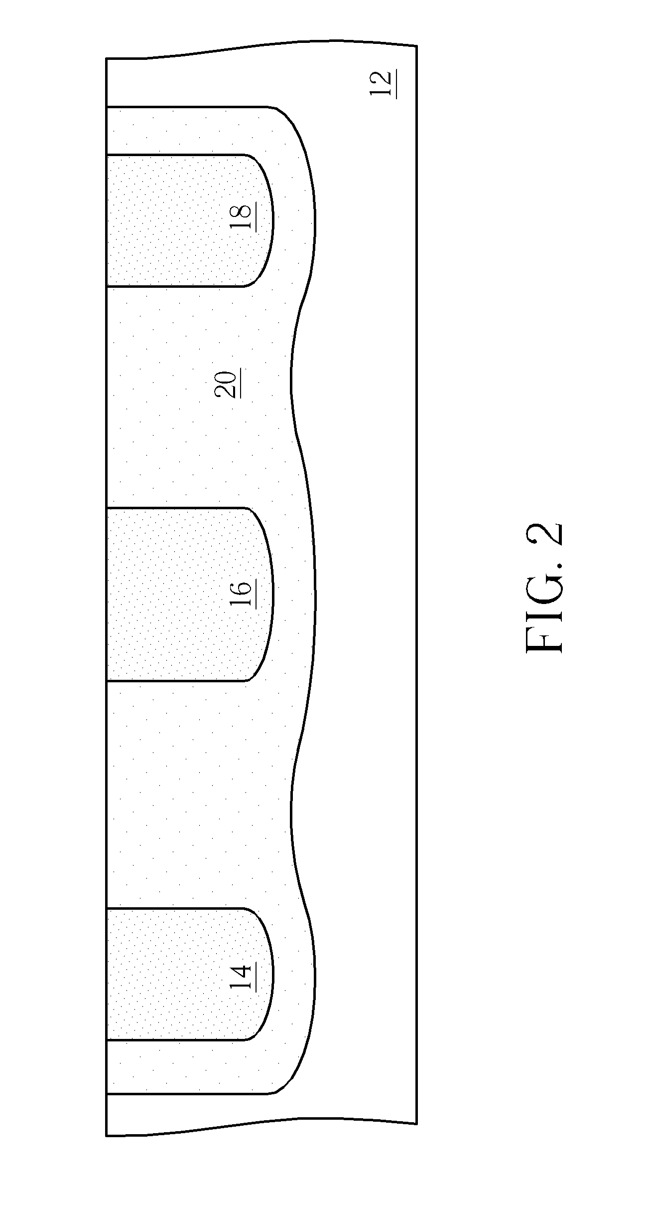
[0015]Referring to FIGS. 1-3, FIGS. 1-3 illustrate a method of fabricating a LDMOS device according to a preferred embodiment of the present invention. It is appreciated that in the drawings and in the following descriptions, a LDMOS device with dual gates is illustrated to highlight the feature of the present invention. However, the following process could also be applied to fabricate a LDMOS device with one single gate, which is also within the scope of the present invention. As shown in FIG. 1, a p-type semiconductor substrate 12 is first provided, and an ion implantation is conducted by using a patterned photoresist (not shown) as mask to implant n-type dopants (such as phosphorus) into the semiconductor substrate 12 for forming a plurality of regions 14, 16, 18. Preferably, the regions 14, 16, 18 formed in the substrate 12 do not contact each other, and it should be noted that despite three regions 14, 16, 18 are formed in the semiconductor substrate 12, the quantity of the reg...


PUM


Abstract

A method for fabricating a lateral-diffusion metal-oxide semiconductor (LDMOS) device is disclosed. The method includes the steps of: providing a semiconductor substrate; forming a first region and a second region both having a first conductive type in the semiconductor substrate, wherein the first region not contacting the second region; and performing a thermal process to diffuse the dopants within the first region and the second region into the semiconductor substrate to form a deep well, wherein the doping concentration of the deep well is less than the doping concentration of the first region and the second region.

Description

BACKGROUND OF THE INVENTION[0001]1. Field of the Invention[0002]The invention relates to a high voltage semiconductor device, and more particularly, to a lateral-diffusion metal-oxide semiconductor (LDMOS) device with high breakdown voltage and low on-state resistance (Ron).[0003]2. Description of the Prior Art[0004]Controllers, memories, circuits of low-voltage operation and power devices of high-voltage operation have been largely integrated together to achieve a single-chip system. The power device, such as vertical double-diffusion metal-oxide-semiconductor (VDMOS), insulated gate bipolar transistor (IGBT) or lateral diffusion MOS (LDMOS), has been employed to increase power switching efficiency and decrease the loss of energy resources. It is often required that the switching transistors withstand high breakdown voltages and operate at a low on-resistance.[0005]Double diffuse drain (DDD) technology has been extensively applied to the source / drain (S / D) in order to provide a hig...

Claims


Application Information

Patent Timeline
IPC IPC(8): H01L29/78H01L21/336
CPCH01L29/0696H01L29/0878H01L29/456H01L29/7816H01L29/665H01L29/66689H01L29/4933
Inventor LIU, TSENG-HSUNLEE, CHIU-LINGCHEN, ZHENG-HONGWANG, YI-MINGLEE, CHING-MING
Owner UNITED MICROELECTRONICS CORP
Why Eureka
Try Eureka