Laminated ceramic electronic component and manufacturing method therefor

a technology of laminated ceramics and electronic components, applied in the direction of fixed capacitor details, fixed capacitors, liquid/solution decomposition chemical coatings, etc., can solve the problem of partially melting copper, achieve the effect of maintaining the surface area ratio of the plating layer, preventing copper from being melted, and maintaining the bonding strength

Active Publication Date: 2011-09-29
MURATA MFG CO LTD
View PDF20 Cites 10 Cited by
  • Summary
  • Abstract
  • Description
  • Claims
  • Application Information

AI Technical Summary

Benefits of technology

[0017]According to a preferred embodiment of the present invention, the average rate of temperature increase from room temperature to the top temperature of about 1000° C. or more is preferably controlled to about 100° C. / minute or more, for example, in the heat treatment step at the temperature of about 1000° C. or more. Thus, the plating layer is prevented from being melted while maintaining the bonding strength between the plating layer and the component main body. Therefore, the surface area ratio of the plating layer is maintained, and the adhesion force to a plating layer provided thereon is further increased.
[0018]Preferably, the plating layer including copper, for example, as its main constituent further increases the bonding strength between the plating layer and the component main body because copper is intrinsically a metal which has good bonding properties to ceramics.

Problems solved by technology

However, the heat treatment performed at a temperature of 1000° C. or more may encounter a problem of the copper being partially melted.

Method used


Image

  • Laminated ceramic electronic component and manufacturing method therefor
  • Laminated ceramic electronic component and manufacturing method therefor
  • Laminated ceramic electronic component and manufacturing method therefor

Examples


Embodiment Construction

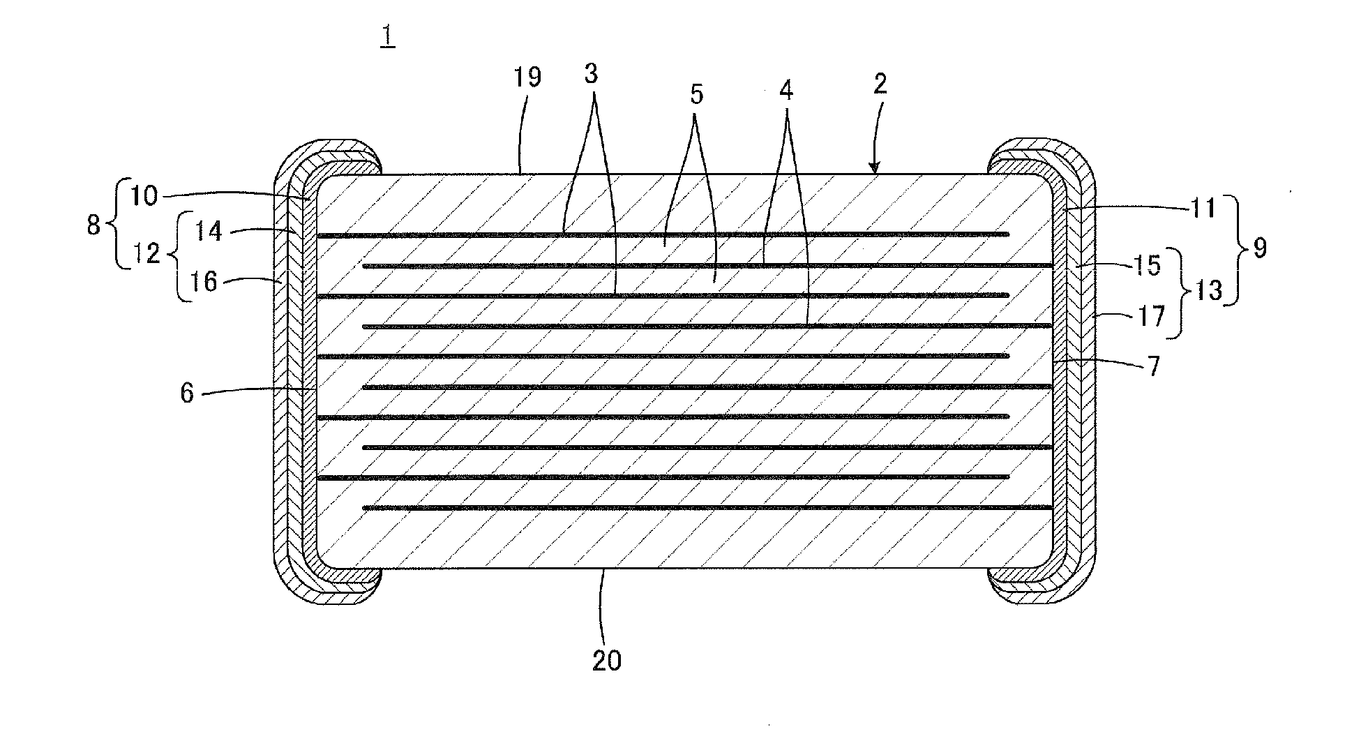
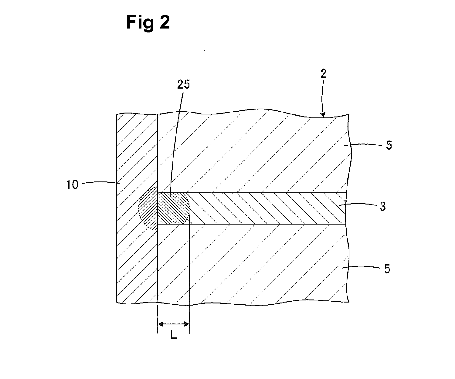
[0024]A laminated ceramic electronic component 1 according to preferred embodiments of the present invention and a manufacturing method therefor will be described with reference to FIGS. 1 and 2.

[0025]The laminated ceramic electronic component 1 preferably includes a component main body 2 having a stacked structure. The component main body 2 includes a plurality of internal electrodes 3 and 4 provided therein. More specifically, the component main body 2 includes a plurality of stacked ceramic layers 5 and a plurality of layered internal electrodes 3 and 4 arranged along the interfaces between the ceramic layers 5. The internal electrodes 3 and 4 preferably include, for example, nickel as a main constituent.

[0026]When the laminated ceramic electronic component 1 defines a laminated ceramic capacitor, the ceramic layers 5 are preferably made of a dielectric ceramic, for example. It is to be noted that the laminated ceramic electronic component 1 may define other components, such as a...


PUM

PropertyMeasurementUnit
temperatureaaaaaaaaaa
eutectic temperatureaaaaaaaaaa
lengthaaaaaaaaaa

Abstract

In a method of forming a plating layer for an external terminal electrode by applying, for example, copper plating to an end surface of a component main body with respective ends of internal electrodes exposed, and then applying a heat treatment at a temperature of about 1000° C. or more in order to improve the adhesion strength and moisture resistance of the external terminal electrode, the plating layer may be partially melted to decrease the bonding strength of the plating layer. In the step of applying a heat treatment at a temperature of about 1000° C. or more to a component main body with plating layers formed thereon, the average rate of temperature increase from room temperature to the temperature of about 1000° C. or more is set to about 100° C. / minute or more. This average rate of temperature increase maintains a moderate eutectic state in the plating layer and ensures a sufficient bonding strength of the plating layer.

Description

BACKGROUND OF THE INVENTION[0001]1. Field of the Invention[0002]The present invention relates to a laminated ceramic electronic component and a manufacturing method therefor, and more particularly, relates to a laminated ceramic electronic component which has an external terminal electrode formed directly by plating so as to be electrically connected to an internal electrode, and a method for manufacturing the laminated ceramic electronic component.[0003]2. Description of the Related Art[0004]As shown in FIG. 3, a laminated ceramic electronic component 101 as typified by a laminated ceramic capacitor includes a component main body 105 including a stack structure including a plurality of stacked ceramic layers 102 made of, for example, a dielectric ceramic, and including a plurality of layered internal electrodes 103 and 104 disposed along the interfaces between the ceramic layers 102. The ends of the plurality of internal electrodes 103 and the ends of the plurality of internal elec...

Claims


Application Information

Patent Timeline
Patent Type & Authority Applications(United States)
IPC IPC(8): H01L41/00H01C7/13H01F5/00H01G4/12C04B33/32H01G4/232H01G4/30
CPCH01G4/005H01G4/30H01G4/12H01G4/228H01G4/248B32B18/00B32B37/18C23C18/40H01G4/012B32B2307/202B32B2315/02B32B2457/00
Inventor MOTOKI, AKIHIROTAKEUCHI, SYUNSUKEOGAWA, MAKOTONISHIHARA, SEIICHIKAWASAKI, KENICHIMATSUMOTO, SHUJI
Owner MURATA MFG CO LTD
Why Eureka
Try Eureka