Low power small area static phase interpolator with good linearity

a static phase interpolator and small area technology, applied in the field of phase interpolators, can solve the problems of large power consumption, large utilization area of current mode logic architecture, and static phase interpolator not providing good linearity

Inactive Publication Date: 2011-10-06
TAIWAN SEMICON MFG CO LTD
View PDF5 Cites 21 Cited by
  • Summary
  • Abstract
  • Description
  • Claims
  • Application Information

AI Technical Summary

Benefits of technology

[0007]Embodiments are provided of a static phase interpolator for providing clock signals of different phases between a first phase of a first clock signal and a second phase of a second clock signal in response to a phase control signal. The static phase interpolator includes a first plurality of inverters coupled in parallel between a first input node for receiving the first clock signal and an output node, and a second plurality of inverters coupled in parallel between a second input node for receiving the second clock signal and the output node. A first plurality of switch elements is coupled to the first plurality of inverters for selectively turning on individual ones of

Problems solved by technology

However, the current mode logic architecture utilizes significant area and suffers from large power consumption.
While the static phase interpolator of FIG.

Method used


Image

  • Low power small area static phase interpolator with good linearity
  • Low power small area static phase interpolator with good linearity
  • Low power small area static phase interpolator with good linearity

Examples


Embodiment Construction

[0018]This description of the exemplary embodiments is intended to be read in connection with the accompanying drawings, which are to be considered part of the entire written description. Relative terms are for convenience of description and do not require that the apparatus be constructed or operated in a particular orientation. Terms concerning communication, coupling and the like, such as “connected” and “interconnected,” refer to a relationship wherein features communicate with one another either directly or indirectly through intervening structures, unless expressly described otherwise.

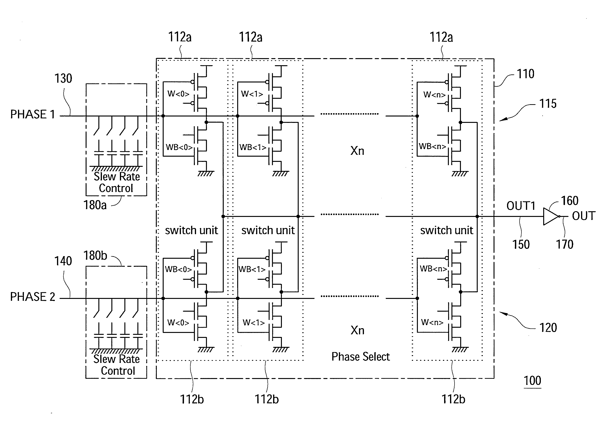
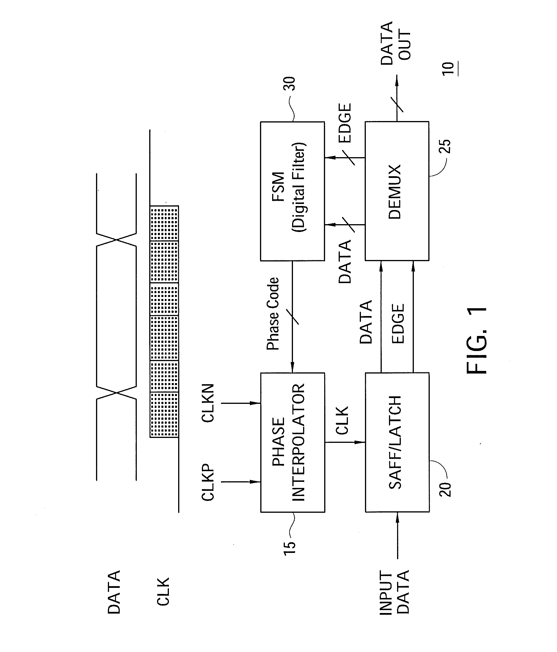
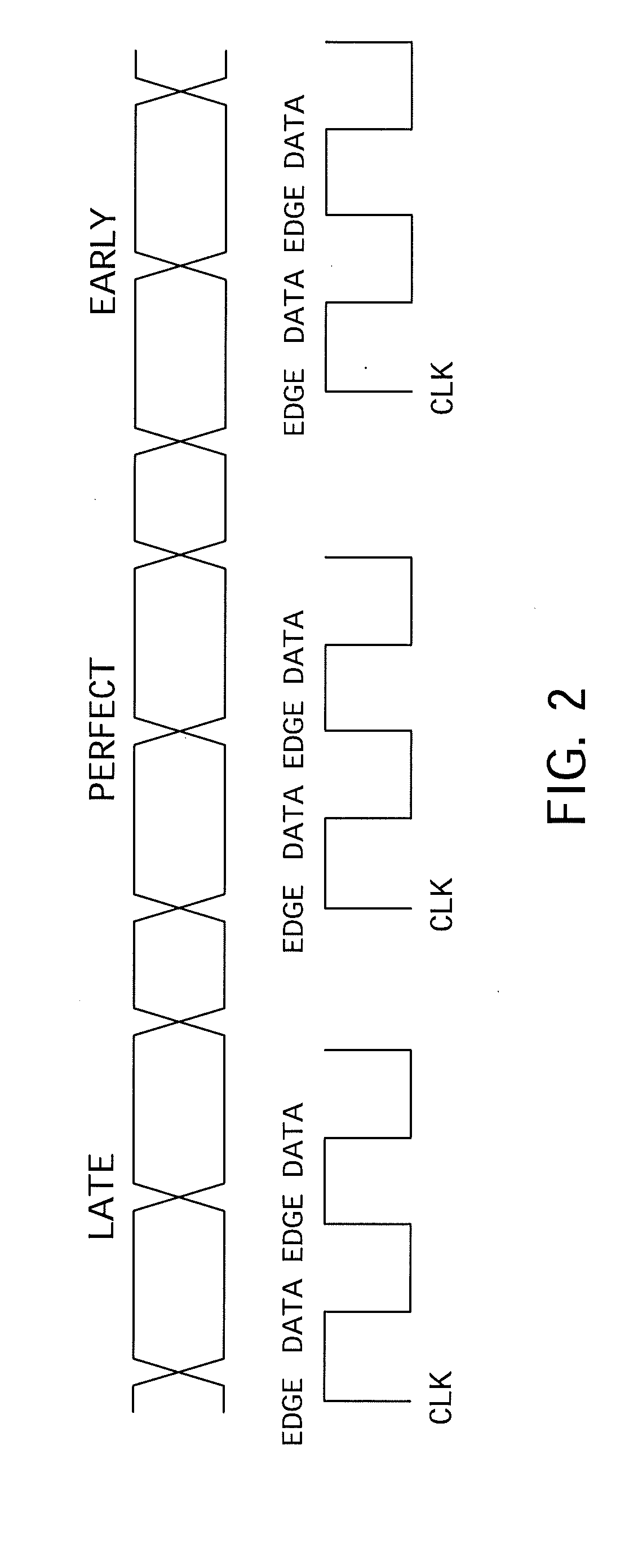
[0019]FIG. 4 is a circuit diagram of an exemplary embodiment of a static phase interpolator 100. FIG. 5 illustrates the configuration of one of the switch units within the static phase interpolator of FIG. 4. FIG. 6 is a timing diagram generally illustrating the operation of a static phase interpolator, such as is shown in FIGS. 3 and 4.

[0020]Referring first to FIG. 4, the static phase interpolat...


PUM


Abstract

A static phase interpolator includes first and second plurality of inverters coupled in parallel between an output node and first and second input nodes for receiving first and second clock signals, and first and second plurality of switch elements coupled to the first and second plurality of inverters for selectively turning on individual ones of the inverters in response to a phase control signal. An inverter is coupled the output node. The interpolator may include a slew rate controller coupled to the first and second input nodes. Also, each inverter of the interpolator may include a PMOS transistor in series with an NMOS transistor and have a respective one of the switch elements disposed between the PMOS and NMOS transistors.

Description

FIELD OF THE INVENTION[0001]The present invention relates to phase interpolators and more particularly top static phase interpolators for use in clock and data recovery circuits.BACKGROUND OF THE INVENTION[0002]Phase interpolators are used in clock and data recovery (CDR) circuits to generate clock signals with different phases and for picking the clock signal having the proper phase. Given two phase inputs (e.g., signals out of phase by 90°), the phase interpolator can provide an output having a phase between the two input phases.[0003]FIG. 1 is a block diagram of a CDR circuit 10. The CDR circuit 10 includes a phase interpolator 15, which receives a pair of clock signals CLKP and CLKN of different phases. The output of the phase interpolator 15 is coupled to a sense amplifier flip flop (SAFF) or alternatively to a latch (together shown as SAFF / Latch 20), which receives as an input the data signal (INPUT DATA) to be recovered. One structure is a CMOS circuit and the other is a curr...

Claims


Application Information

Patent Timeline
IPC IPC(8): H03H11/26
CPCH03K2005/00286H03H11/265
Inventor FU, CHIN-MING
Owner TAIWAN SEMICON MFG CO LTD
Why Eureka
Try Eureka