Manufacturing method of semiconductor chip-embedded wiring substrate

a manufacturing method and technology of wiring substrate, applied in the direction of solid-state devices, printed circuit aspects, basic electric elements, etc., can solve the problems of difficult to ensure the sufficient amount of conductive particles, difficult to form via holes, etc., and achieve the effect of shortening the manufacturing time and simplifying the manufacturing process

Inactive Publication Date: 2011-10-06
DENSO CORP
View PDF2 Cites 59 Cited by
  • Summary
  • Abstract
  • Description
  • Claims
  • Application Information

AI Technical Summary

Benefits of technology

[0010]In view of the above-described problem, it is an object of the present invention to provide a manufacturing method o

Problems solved by technology

Therefore, it becomes difficult to form a via hole and fill a via hole with conductive paste by the above-described method.
Moreover, since the amount of conductive paste to be filled is sma

Method used


Image

  • Manufacturing method of semiconductor chip-embedded wiring substrate
  • Manufacturing method of semiconductor chip-embedded wiring substrate
  • Manufacturing method of semiconductor chip-embedded wiring substrate

Examples


first embodiment

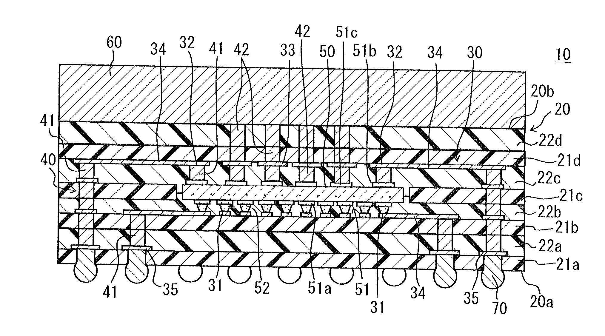
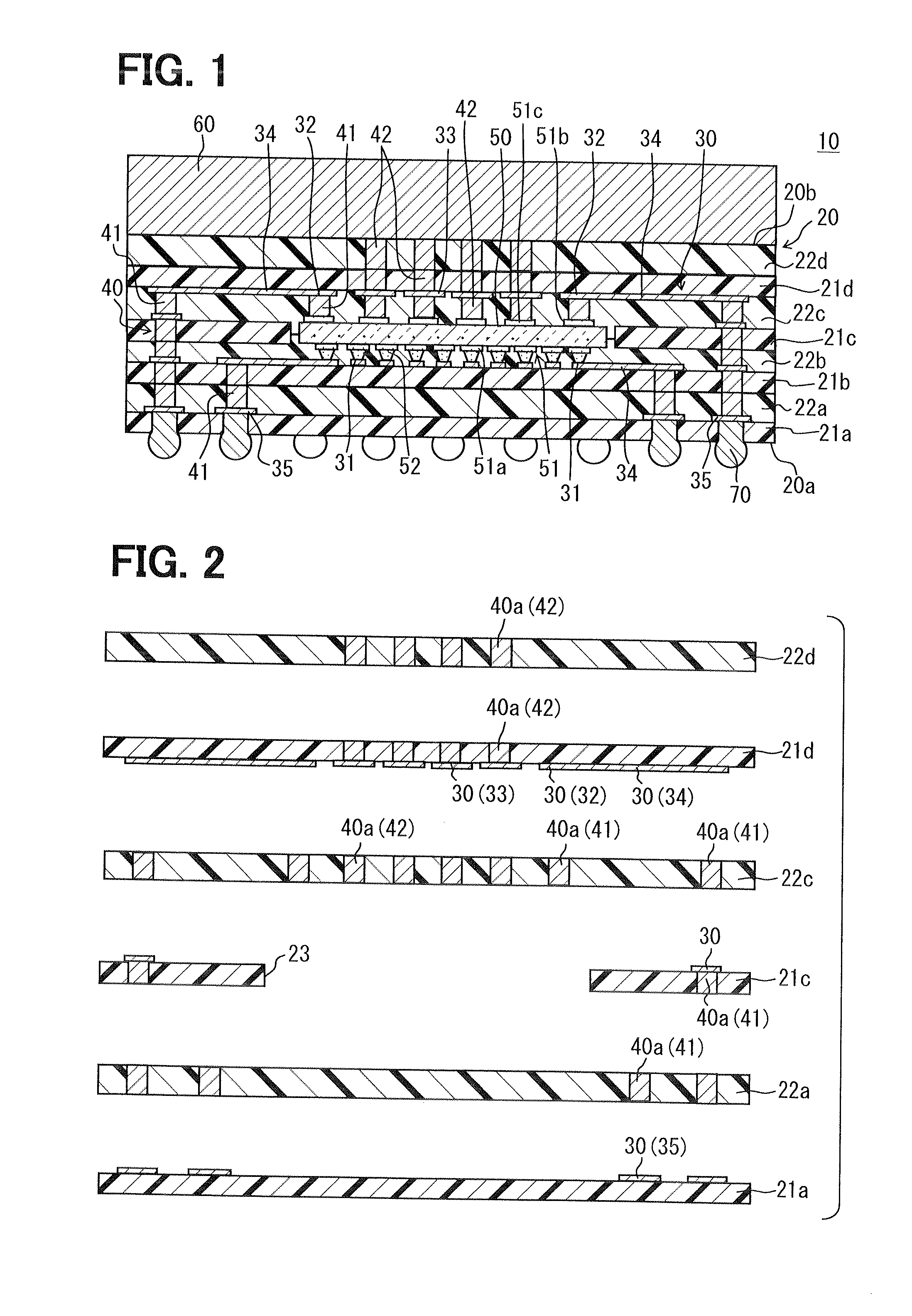
[0038]Hereinafter, embodiments of the present invention will be described with reference to drawings. A thickness direction of an insulating substrate 20 (in other words, a stacking direction of multiple resin films) is referred to as a thickness direction, and a direction perpendicular to the thickness direction is referred to as a perpendicular direction. In addition, a thickness indicates a thickness along the thickness direction, unless otherwise noted.

[0039]A semiconductor chip-embedded wiring substrate 10 (i.e., semiconductor device hereinafter referred to as a wiring substrate 10) shown in FIG. 1 includes the insulating substrate 20, a conductive pattern 30 and an interlayer connecting portion 40 which are formed in the insulating substrate 20, and a semiconductor chip 50 which is buried, that is, embedded in the insulating substrate 20, as basic components of a semiconductor chip-embedded wiring substrate. In addition to the above-described components, the wiring substrate 1...

second embodiment

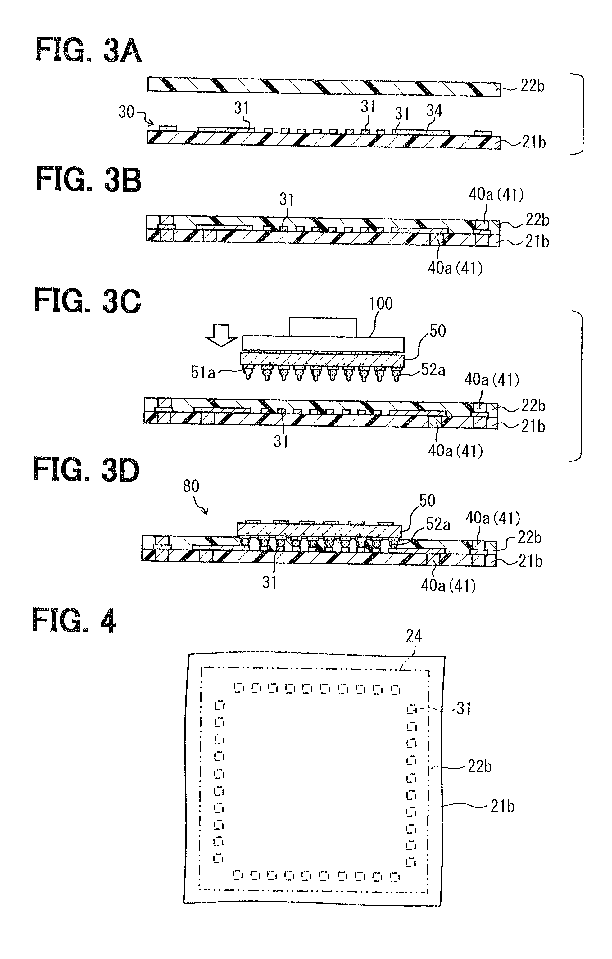
[0144]In the first embodiment, when the semiconductor chip 50 is flip-chip mounted on the thermosetting resin film 21b as the substrate, the stud bump 52a is stuffed into the thermoplastic resin film 22b attached to the pad formation surface of the thermosetting resin film 21b to secure the pressure welding state with the pad 31.

[0145]In contrast, in the present embodiment, as shown in FIGS. 7A and 7B, a through-hole 25 is formed in the thermoplastic resin film 22b at a position corresponding to the pad 31, and the thermoplastic resin film 22b is attached to the pad formation surface of the thermosetting resin film 21b such that the through-hole 25 covers the pad 31.

[0146]In the example shown in FIGS. 7A and 7B, each of the multiple through-holes 25 is formed for the corresponding one pad 31. Accordingly, since the thermoplastic resin film 22b is located between the adjacent connecting portions, each of which is formed between the stud bump 52a and the pad 31, it is easy for the sof...


PUM


Abstract

With respect to a substrate including a first film, on a surface of which a pad is formed, a second film made of thermoplastic resin is a thermal compression bonded to a pad formation surface of the substrate. A stud bump formed on a semiconductor chip is stuffed into the second film while melting the second film and is pressure welded to the pad by application of pressure and heat. The melted second film seals between the semiconductor chip and the substrate. Then, multiple resin films are stacked with the substrate and the second film to form a stacked body. In a pressurizing and heating process, the multiple resin films, the substrate and the second film are integrated at one time so that the stud bump is bonded to the pad.

Description

CROSS REFERENCE TO RELATED APPLICATION[0001]The present application is based on Japanese Patent Application No. 2010-86348 filed on Apr. 2, 2010, the disclosure of which is incorporated herein by reference.FIELD OF THE INVENTION[0002]The present invention relates to a manufacturing method of a semiconductor chip-embedded wiring substrate.BACKGROUND OF THE INVENTION[0003]Conventionally, as a manufacturing method of a component-embedded substrate, in which a wiring part is formed and an electronic component is embedded in an insulating substrate including thermoplastic resin, a method described in JP-A-2007-324550 corresponding to US 2008 / 017409 is well known.[0004]According to the manufacturing method, multiple resin films including a resin film having a conductive pattern on a surface thereof and a resin film having a via hole filled with conductive paste are stacked such that the electronic component is embedded and a stacked body is formed.[0005]Then, the stacked body is pressuriz...

Claims


Application Information

Patent Timeline
IPC IPC(8): H01L21/56
CPCH01L21/56H01L23/3107H01L23/49822H01L23/5389H01L24/13H01L24/16H01L24/73H01L24/75H01L24/81H01L24/83H01L2224/0401H01L2224/05624H01L2224/13144H01L2224/16225H01L2224/73204H01L2224/73259H01L2224/7525H01L2224/81203H01L2224/81447H01L2224/83192H01L2924/01013H01L2924/01029H01L2924/01033H01L2924/01047H01L2924/01079H01L2924/01082H01L2924/15311H05K1/0206H05K1/186H01L2924/01005H01L2924/01006H01L2924/01019H01L2924/0105H01L2924/01068H01L2924/014H05K2201/066H01L2924/13091H01L2224/32225H01L2924/13055H01L2924/10253H01L2924/00H01L2924/3512H01L2224/05644H01L2224/05655H01L2224/06135H01L2924/14H01L2924/00014H01L2924/013
Inventor KONDO, KENJI
Owner DENSO CORP
Why Eureka
Try Eureka