Semiconductor device manufacturing method

Active Publication Date: 2011-10-06
MITSUMI ELECTRIC CO LTD
View PDF12 Cites 23 Cited by
  • Summary
  • Abstract
  • Description
  • Claims
  • Application Information

AI Technical Summary

Benefits of technology

[0014]An object of an embodiment of the present invention is to provide a semiconductor device manufacturing method by which

Problems solved by technology

The void 370 may cause the resistance of the contact part 330 to increase and/or adversely affect the electrode reliability.
However, in this configuration, since all the dielectric film h

Method used


Image

  • Semiconductor device manufacturing method
  • Semiconductor device manufacturing method
  • Semiconductor device manufacturing method

Examples


Embodiment Construction

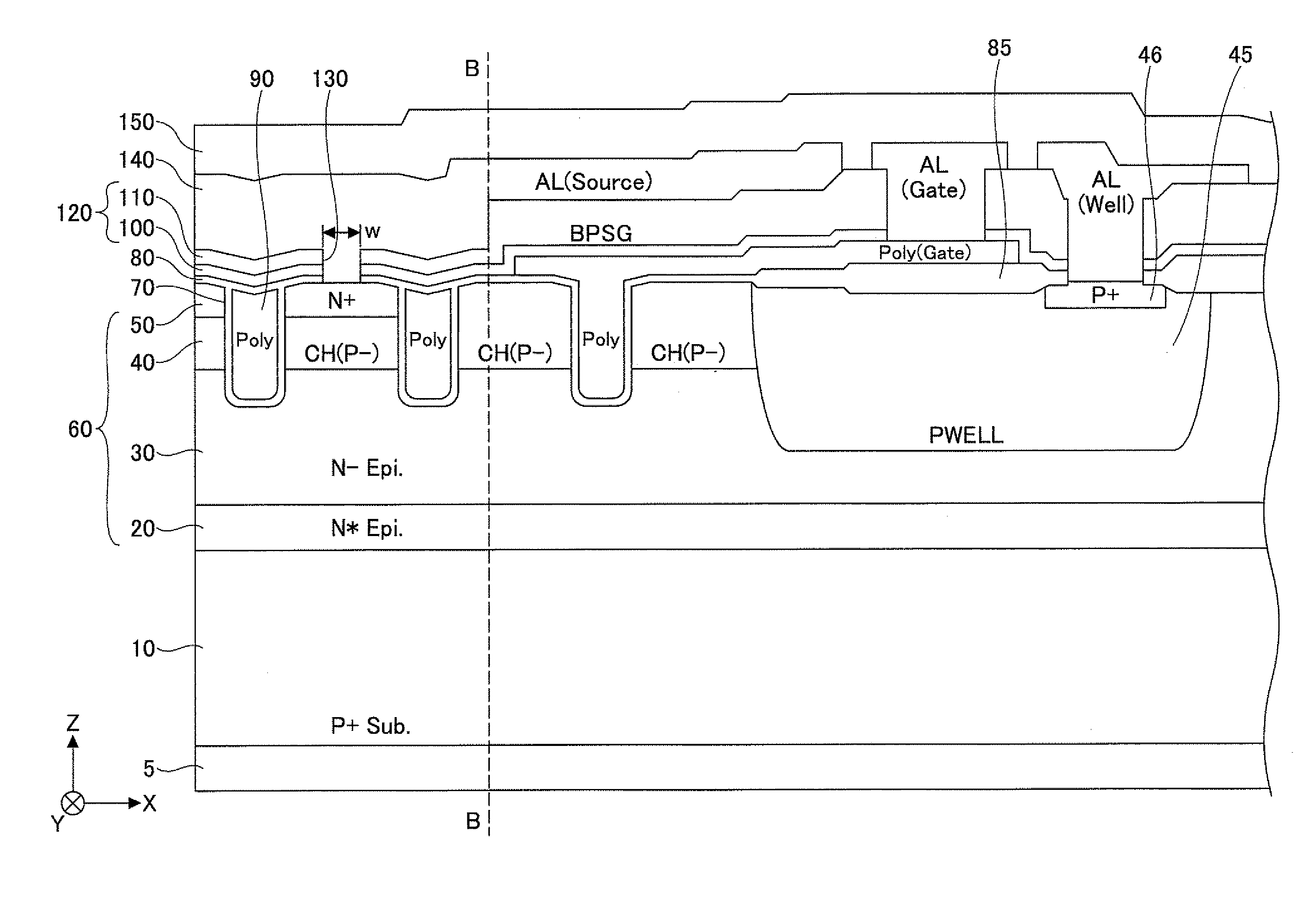
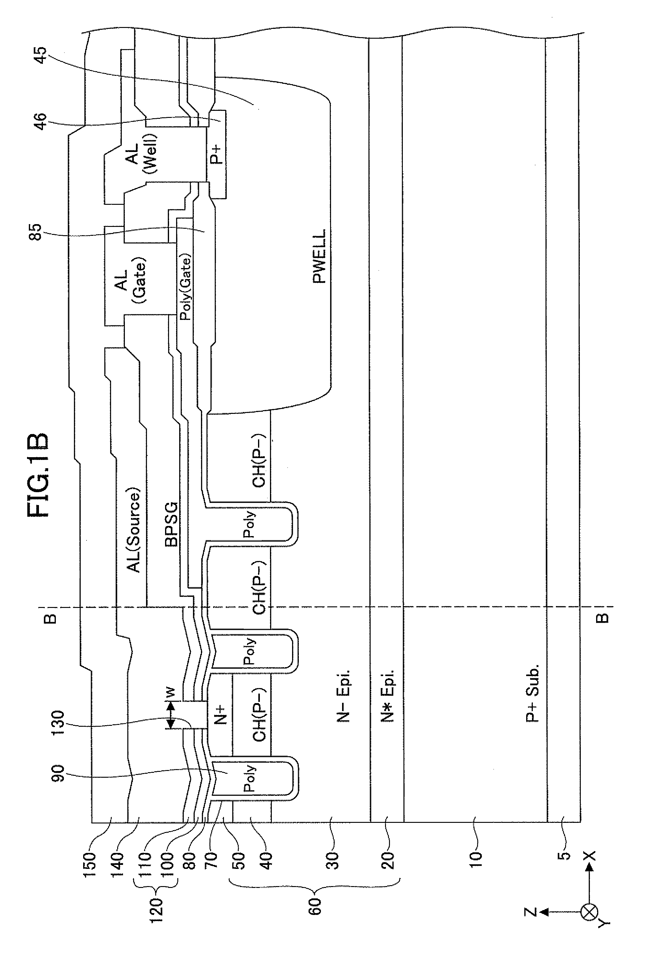
[0027]Below, an embodiment of the present invention will be described with reference to figures.

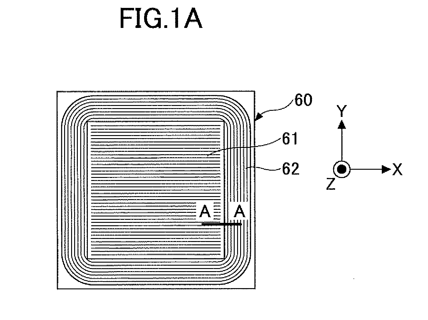
[0028]In FIG. 1A, a semiconductor device according to the embodiment includes a semiconductor layer 60 formed on a semiconductor substrate 10. The semiconductor layer 60 includes a cell part 61 and a guard ring part 62. The cell part 61 is an area in which plural transistor cells are formed. In the cell part 61, the plural transistor cells are formed, and all of the plural transistor cells form a single transistor. The guard ring part 62 is an area for electrically connecting the individual elements of the transistor cells included in the cell part 61 and connecting them with the outside, for causing the plural transistor cells to collectively operate as the single transistor. The guard ring part 62 is formed to surround the periphery of the cell part 61.

[0029]FIG. 1B shows a sectional view taken along a line A-A shown in FIG. 1A. A B-B line extending in a vertical direction in FIG. 1B re...


PUM


Abstract

A semiconductor device manufacturing method is a method of forming a semiconductor device that includes a cell part that includes plural transistor cells in each of which a gate of a trench type is formed in a semiconductor layer, and diffused layers are formed on both sides of the gate, and a guard ring part that surrounds the cell part. The semiconductor device manufacturing method includes forming an interlayer dielectric film on a surface of the semiconductor layer in which the gate and the diffused layers are formed; reducing a thickness of the interlayer dielectric film formed in the cell part through etch back; forming a contact part having a shape of a hole or a groove in the interlayer dielectric film at a position above the diffused layer; and forming a metal film on the interlayer dialectic film.

Description

BACKGROUND OF THE INVENTION[0001]1.Field of the Invention[0002]The present invention relates to a semiconductor device manufacturing method, and in particular, to a semiconductor device manufacturing method of manufacturing a semiconductor device in which a trench-type gate is formed in a semiconductor layer.[0003]2. Description of the Related Art[0004]A trench-type IGBT (Insulated Gate Bipolar Transistor) is known in which a trench is formed in a semiconductor layer formed on a semiconductor substrate, a gate is formed as a result of a polysilicon film being embedded after an oxide film has been formed in the trench, and diffused layers are formed on both sides of the gate.[0005]FIG. 6 shows a sectional view of one example of the trench-type IGBT. In FIG. 6, on a p-type semiconductor substrate 210, a high-concentration n-type epitaxial layer 220 and a low-concentration n-type epitaxial layer 230 are laminated. On the surface of the low-concentration n-type epitaxial layer 230, a p ...

Claims


Application Information

Patent Timeline
IPC IPC(8): H01L21/3205H01L21/332H01L21/336
CPCH01L29/402H01L29/7397H01L29/66348H01L29/42376
Inventor KIKUCHI, HIROAKIKONDO, KATSUNORISHINOHARA, SHIGERUTAKAHASHI, OSAMUYAMABAYASHI, TOMOAKI
Owner MITSUMI ELECTRIC CO LTD
Why Eureka
Try Eureka