Pixel structure of organic light emitting diode display and manufacturing method thereof

a technology of light-emitting diodes and pixel structures, which is applied in the direction of thermoelectric device junction materials, electrical devices, semiconductor devices, etc., to achieve the effect of fast switching ra

Active Publication Date: 2011-10-13
AU OPTRONICS CORP
View PDF9 Cites 18 Cited by
  • Summary
  • Abstract
  • Description
  • Claims
  • Application Information

AI Technical Summary

Benefits of technology

[0010]The present invention utilizes the first SS of the first transistor being smaller than the second SS of the second transistor to differentiate the current-voltage characteristics of the first transistor and the second transistor, so that the first transistor can have a faster switching rate, and the second transistor can provide various values of the second drain current.

Problems solved by technology

However, when the driving transistor and the switching transistor have the same SS, the switching transistor cannot turn on the driving transistor rapidly, so that the OLED display easily generates residual images.

Method used


Image

  • Pixel structure of organic light emitting diode display and manufacturing method thereof
  • Pixel structure of organic light emitting diode display and manufacturing method thereof
  • Pixel structure of organic light emitting diode display and manufacturing method thereof

Examples


Embodiment Construction

[0021]To provide a better understanding of the present invention, preferred embodiments will be detailed as follows. The preferred embodiments of the present invention are illustrated in the accompanying drawings with numbered elements to elaborate the contents and effects to be achieved.

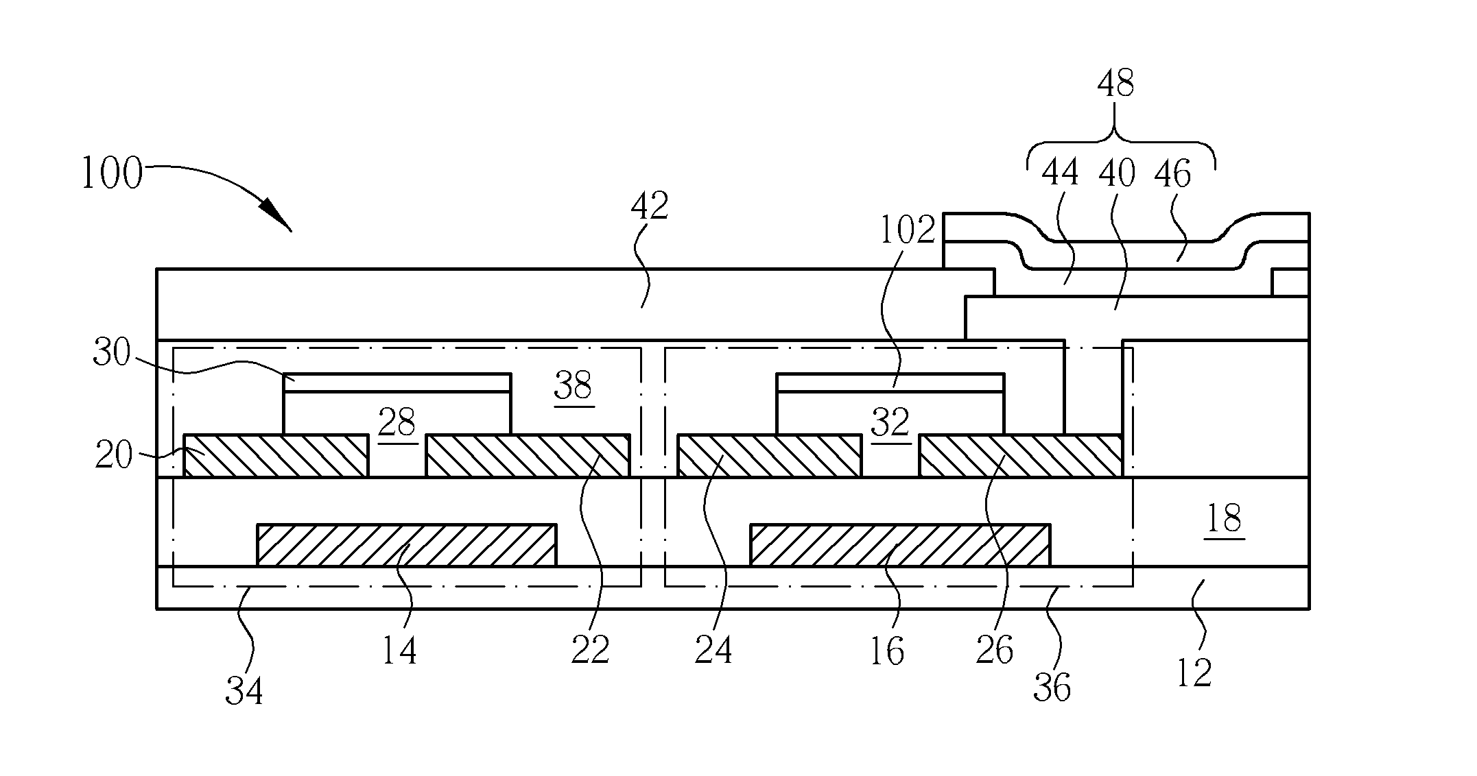
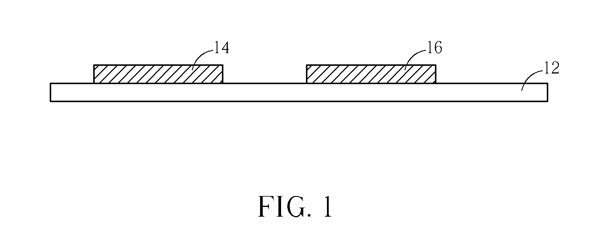
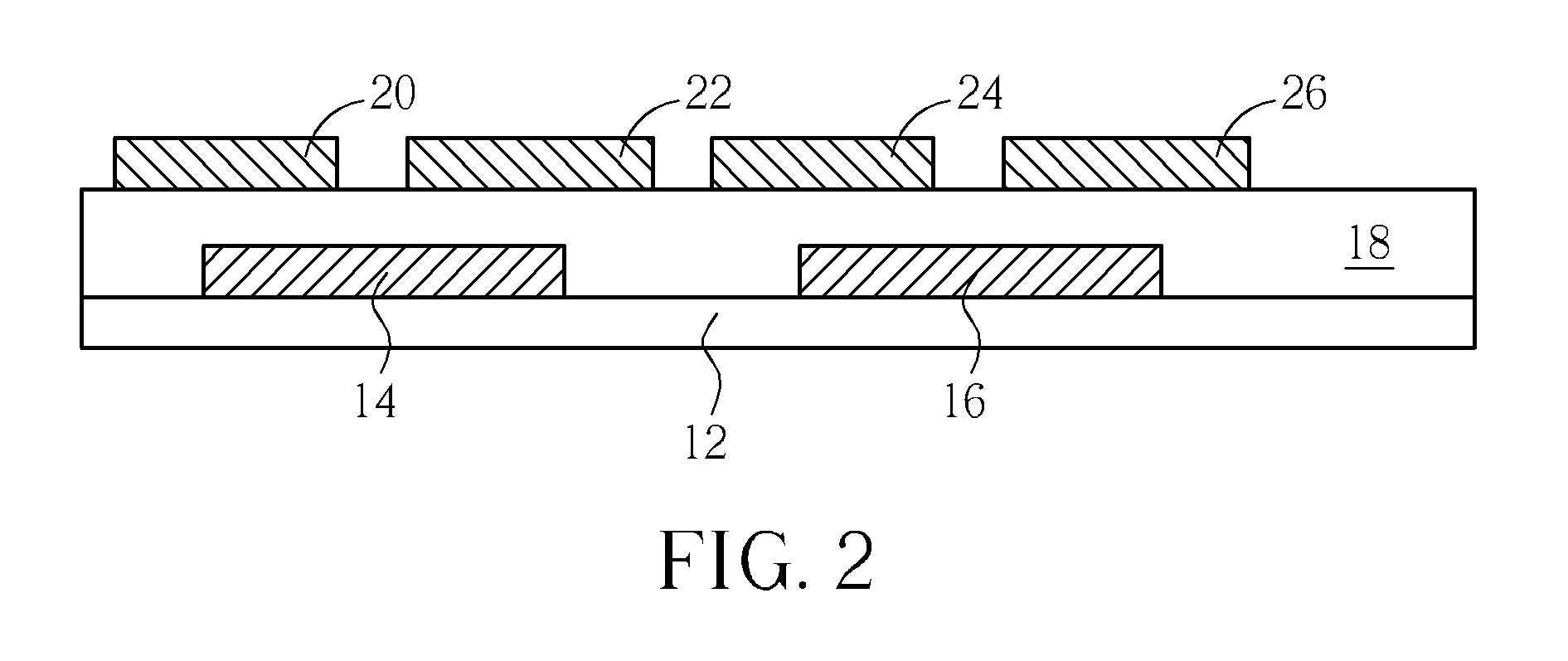
[0022]Refer to FIG. 1 through FIG. 5, which are schematic diagrams illustrating a manufacturing method of a pixel structure of an organic light emitting diode (OLED) display according to a first preferred embodiment of the present invention. As shown in FIG. 1, a substrate 12 is provided first. The substrate 12 can be any kind of substrate for manufacturing thin film transistors, such as a silicon substrate, a glass substrate or a plastic substrate, etc. Then, a first metal layer is formed on the substrate 12. A first photolithographic and etching process is then performed to pattern the first metal layer, so that a first gate electrode 14 and a second gate electrode 16 are formed. The first gate el...


PUM


Abstract

A pixel structure of an organic light emitting diode display includes a first transistor and a second transistor. The first transistor includes a first drain electrode and a first source electrode. When a voltage difference is provided between the first drain electrode and the first source electrode, the first transistor has a first subthreshold slope (SS). The second transistor includes a second drain electrode and a second source electrode. When the voltage difference is provided between the second drain electrode and the second source electrode, the second transistor has a second SS, and the second SS is larger than the first SS.

Description

BACKGROUND OF THE INVENTION[0001]1. Field of the Invention[0002]The present invention relates to a pixel structure of an organic light emitting diode display and a manufacturing method thereof, and more particularly, to a pixel structure of an organic light emitting diode display having two diodes with different current-voltage characteristics.[0003]2. Description of the Prior Art[0004]Recently, organic light emitting diode (OLED) displays have become popular flat displays because of having the advantages of self-luminescence, wide viewing angle, fast response time, high illumination efficiency, low operating voltage, thin panel thickness, flexibility and a simple fabricating process, and thus, the OLED displays have been widely applied to various kinds of flat display products.[0005]A pixel structure of the OLED display includes an OLED, a driving transistor and a switching transistor. The driving transistor is electrically connected to the organic OLED so as to control a switch of...

Claims


Application Information

Patent Timeline
Patent Type & Authority Applications(United States)
IPC IPC(8): H01L51/52H01L51/56
CPCH01L27/1214H01L27/3244H01L27/1251H01L27/1225H10K59/12
Inventor HSIEH, HSING-HUNG
Owner AU OPTRONICS CORP
Why Eureka
Try Eureka