Preferential dielectric gapfill

a dielectric gap and dielectric technology, applied in the direction of basic electric elements, electric apparatus, semiconductor/solid-state device manufacturing, etc., can solve the problem of rarely desirable etching, and achieve the effect of rapid etching

Active Publication Date: 2011-10-13
APPLIED MATERIALS INC
View PDF11 Cites 10 Cited by
  • Summary
  • Abstract
  • Description
  • Claims
  • Application Information

AI Technical Summary

Benefits of technology

[0006]Aspects of the disclosure pertain to methods of preferentially filling narrow trenches with silicon oxide while not completely filling wider trenches and / or open areas. In embodiments, dielectric layers are deposited by flowing a silicon-containing precursor and ozone into a processing chamber such that a relatively dense first portion of a silicon oxide layer followed by a more porous (and more rapidly etched) second portion of the silicon oxide layer. Narrow trenches are filled with dense material whereas open areas are covered with a layer of dense material and more porous material. Dielectric material in wider trenches may be removed at this point with a wet etch while the dense material in narrow trenches is retained.

Problems solved by technology

Dishing is rarely desirable since the material in the open area is not completely removed nor is it flush with the level of the silicon oxide in the narrow trench.

Method used


Image

  • Preferential dielectric gapfill
  • Preferential dielectric gapfill
  • Preferential dielectric gapfill

Examples


Embodiment Construction

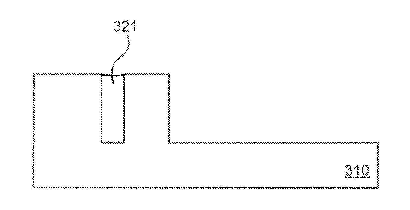
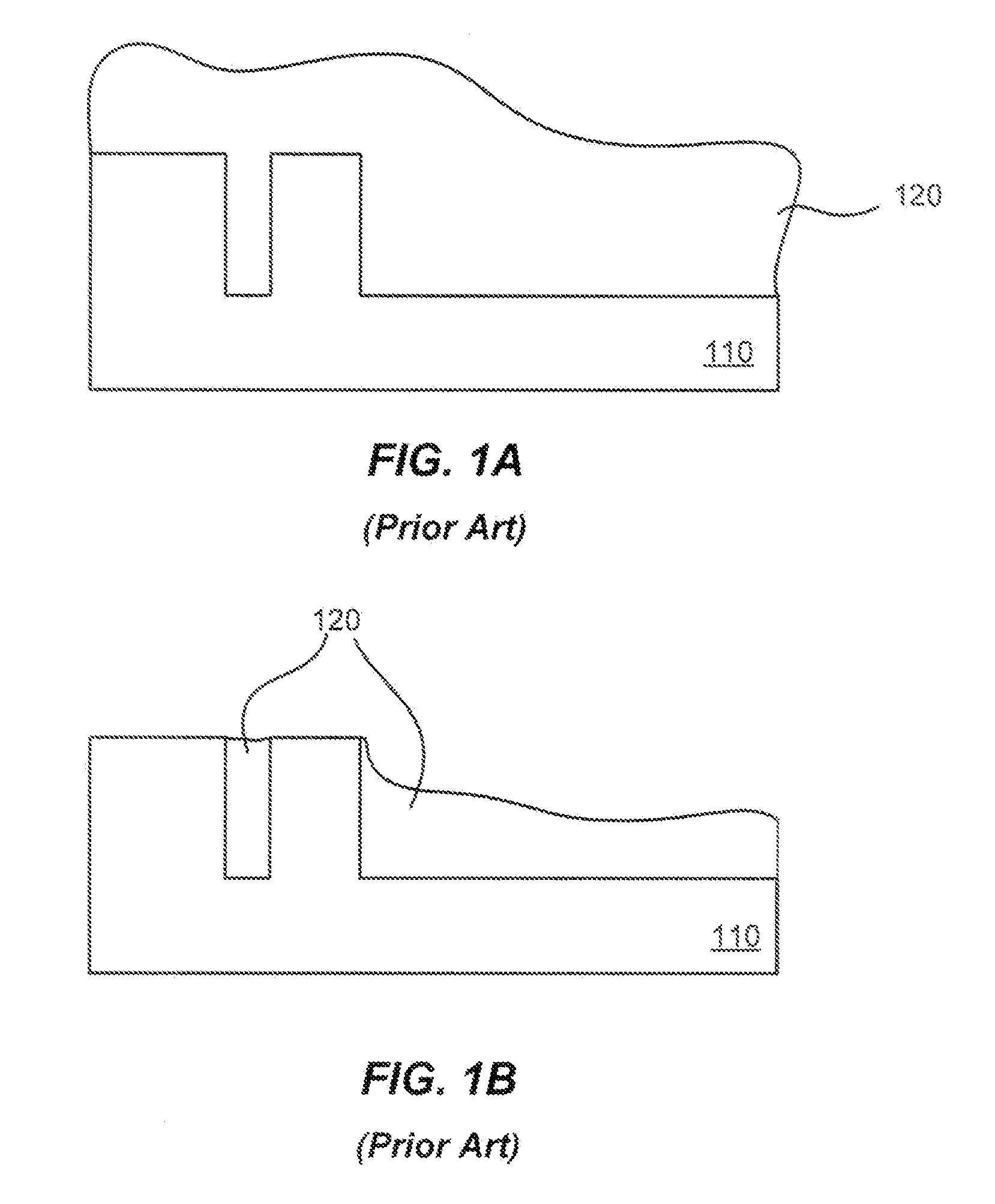
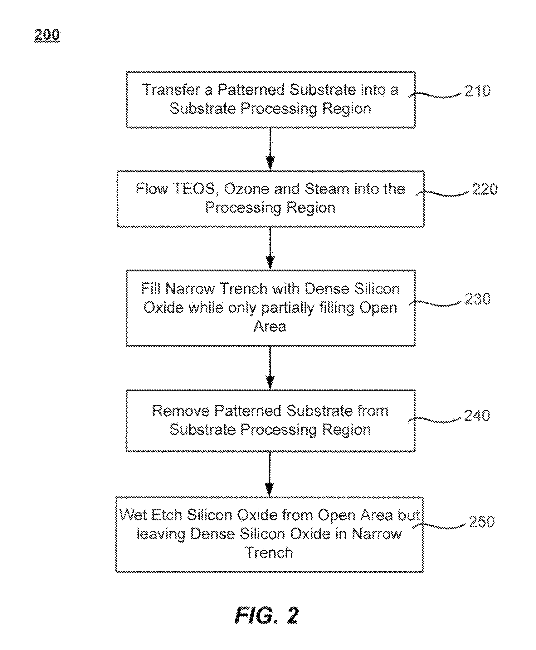
[0016]Aspects of the disclosure pertain to methods of preferentially filling narrow trenches with silicon oxide while not completely filling wider trenches and / or open areas. In embodiments, dielectric layers are deposited by flowing a silicon-containing precursor and ozone into a processing chamber such that a relatively dense first portion of a silicon oxide layer followed by a more porous (and more rapidly etched) second portion of the silicon oxide layer. Narrow trenches are filled with dense material whereas open areas are covered with a layer of dense material and more porous material. Dielectric material in wider trenches may be removed at this point with a wet etch while the dense material in narrow trenches is retained.

[0017]Embodiments of the invention are directed to methods of forming silicon oxide preferentially in narrow trenches on a patterned surface of a substrate. Sub-atmospheric CVD (SACVD) and related processes involve flowing a silicon-containing precursor and a...


PUM

PropertyMeasurementUnit
widthaaaaaaaaaa
depthaaaaaaaaaa
temperatureaaaaaaaaaa

Abstract

Aspects of the disclosure pertain to methods of preferentially filling narrow trenches with silicon oxide while not completely filling wider trenches and/or open areas. In embodiments, dielectric layers are deposited by flowing a silicon-containing precursor and ozone into a processing chamber such that a relatively dense first portion of a silicon oxide layer followed by a more porous (and more rapidly etched) second portion of the silicon oxide layer. Narrow trenches are filled with dense material whereas open areas are covered with a layer of dense material and more porous material. Dielectric material in wider trenches may be removed at this point with a wet etch while the dense material in narrow trenches is retained.

Description

CROSS-REFERENCES TO RELATED APPLICATIONS[0001]This application claims the benefit of U.S. Provisional Application No. 61 / 322,958 by Kweskin et al, filed Apr. 12, 2010 and titled “PREFERENTIAL DIELECTRIC GAPFILL” which is incorporated herein in its entirety for all purposes.BACKGROUND OF THE INVENTION[0002]Semiconductor device geometries continue to decrease in size, providing more devices per unit area on a fabricated wafer. These devices are typically initially isolated from each other as they are built into the wafer, and they are subsequently interconnected to create desired circuit configurations. Some devices are fabricated with feature dimensions of several tens of nanometers. Spacing between doped-semiconductor devices and conductive lines on a patterned wafer may be separated by spacings similar to feature dimensions, leaving recesses or gaps of a comparable size. A nonconductive layer of dielectric material, such as silicon oxide (SiO2), is typically deposited over features...

Claims


Application Information

Patent Timeline
Patent Type & Authority Applications(United States)
IPC IPC(8): H01L21/762
CPCH01L21/76229H01L21/67017
Inventor KWESKIN, SASHAHAMANA, HIROSHIGEE, PAUL EDWARDVENKATARAMAN, SHANKARSAPRE, KADAR
Owner APPLIED MATERIALS INC
Why Eureka
Try Eureka