

Method of polishing wafer surface on which copper and silicon are exposed
a technology of polishing composition and wafer surface, which is applied in the direction of electrical equipment, metal-working equipment, lapping machines, etc., can solve the problems of contaminating the wafer with copper, using polishing compositions, and degrading the electric characteristics of semiconductor devices, so as to prevent copper contamination
- Summary
- Abstract
- Description
- Claims
- Application Information
AI Technical Summary
Benefits of technology
Problems solved by technology
Method used
Image

Examples
Embodiment Construction
[0010]Hereinafter, one embodiment of the present invention will be described.
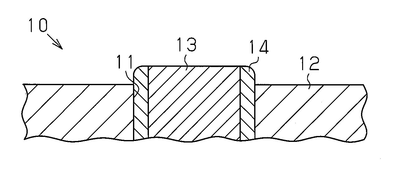
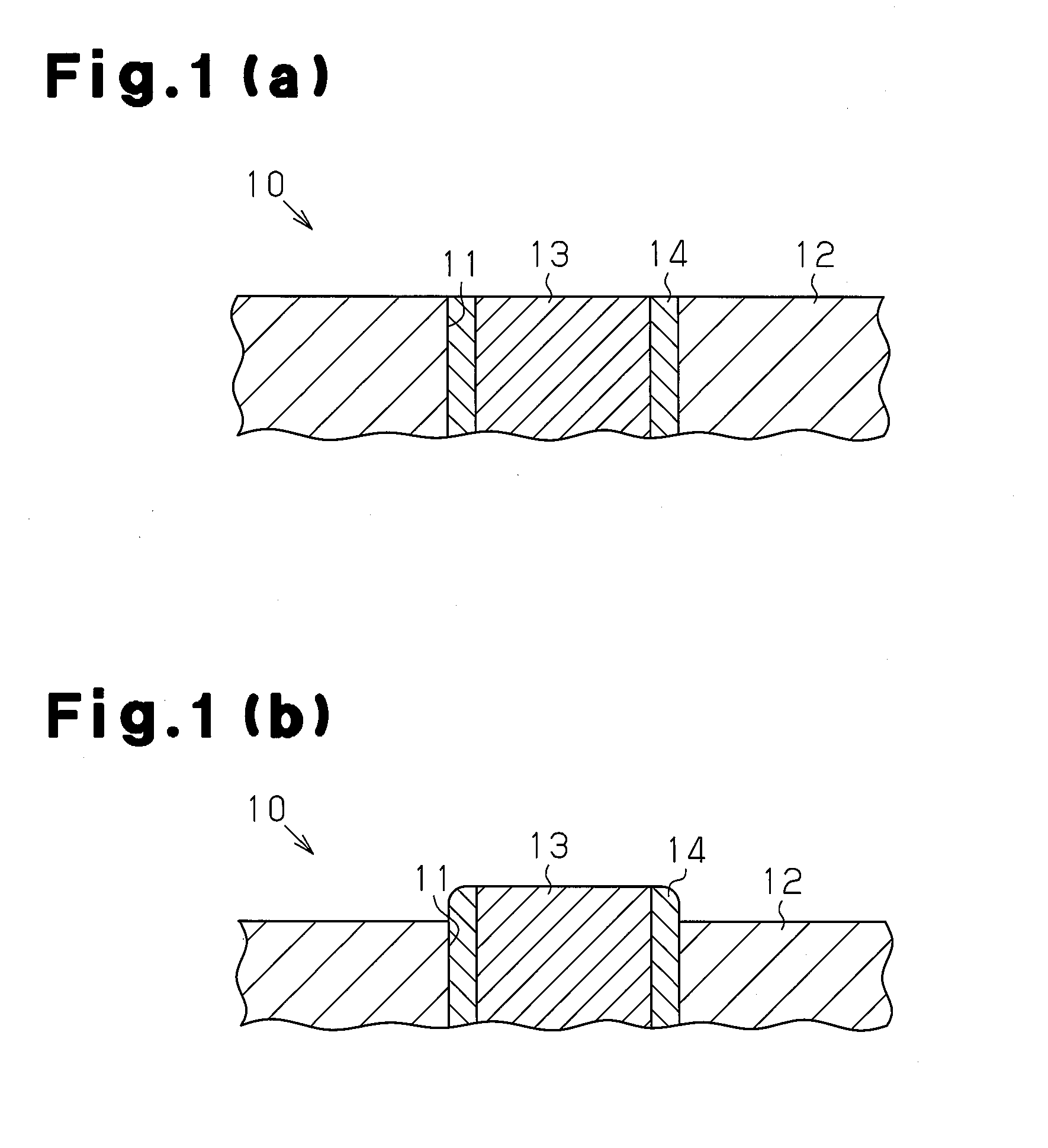
[0011]In a polishing method of the present embodiment, a wafer having an exposed copper or copper alloy surface and an exposed silicon surface is subjected to chemical mechanical polishing using a polishing composition. A wafer 10 shown in FIG. 1(a) comprises a silicon substrate 12 having a via 11 and a conductor 13 composed of copper or a copper alloy with which the via 11 is filled. The wafer 10 has an exposed copper or copper alloy surface and an exposed silicon surface. A barrier metal film 14 is provided on the surface defining the via 11 and prevents the diffusion of copper atoms of the conductor 13 to the silicon substrate 12. The barrier metal film 14 is formed, for example, from tantalum, tantalum nitride, or titanium nitride.
[0012]The chemical mechanical polishing of a wafer having an exposed copper or copper alloy surface and an exposed silicon surface is performed, for example, for planarizing t...
PUM
| Property | Measurement | Unit |
|---|---|---|
| pH | aaaaa | aaaaa |
| pH | aaaaa | aaaaa |
| temperature | aaaaa | aaaaa |
Abstract
Description
Claims
Application Information