Semiconductor device and method of manufacturing the same

a semiconductor and device technology, applied in the direction of semiconductor devices, radio frequency controlled devices, electrical devices, etc., can solve the problems of disadvantageous degrading the carrier mobility of the channel region, avoid the growth of the interface layer and the degradation of the carrier mobility, and reduce the eot of the device. , the effect of reducing the eo

Active Publication Date: 2011-10-20
INST OF MICROELECTRONICS CHINESE ACAD OF SCI
View PDF2 Cites 31 Cited by
  • Summary
  • Abstract
  • Description
  • Claims
  • Application Information

AI Technical Summary

Benefits of technology

[0007]By forming a multi-component high-k interface layer containing elements of the substrate from an ultra-thin high-k dielectric material in a single-layer structure of atoms by rapid annealing, and forming a high-k gate dielectric layer with a higher dielectric constant thereon, the present invention may effectively reduce the EOT of the device, and prevent the diffusion of atoms in the high-k gate dielectric layer from an upper level thereof at high-temperature treatment by the optimized high-k interface layer. Thus, the present invention advantageously avoids growth of the interface layers and degradation of carrier mobility. Furthermore, the present invention may further alleviate the problem of high interface state and interface roughness caused by direct contact of the high-k gate dielectric layer with high dielectric constant and the substrate, and thus the overall performance of the device is effectively enhanced.

Problems solved by technology

With the continuous thinning of the interface layer, some atoms in the high-k gate dielectric material may be diffused into the channel region of the semiconductor substrate through the ultra-thin interface layer in high-temperature thermal treatment, which may disadvantageously degrade the carrier mobility of the channel region.

Method used


Image

  • Semiconductor device and method of manufacturing the same
  • Semiconductor device and method of manufacturing the same
  • Semiconductor device and method of manufacturing the same

Examples


Embodiment Construction

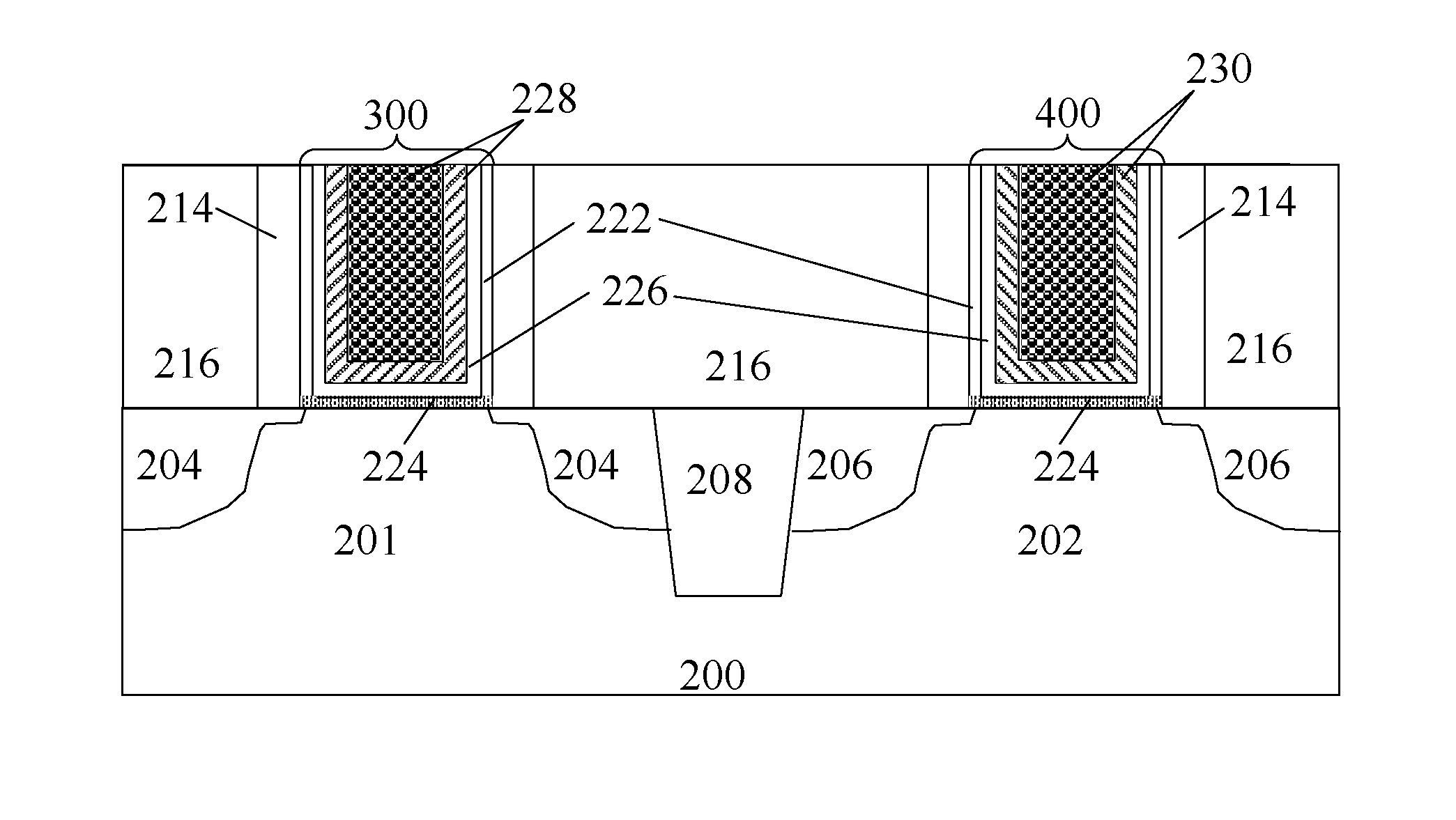
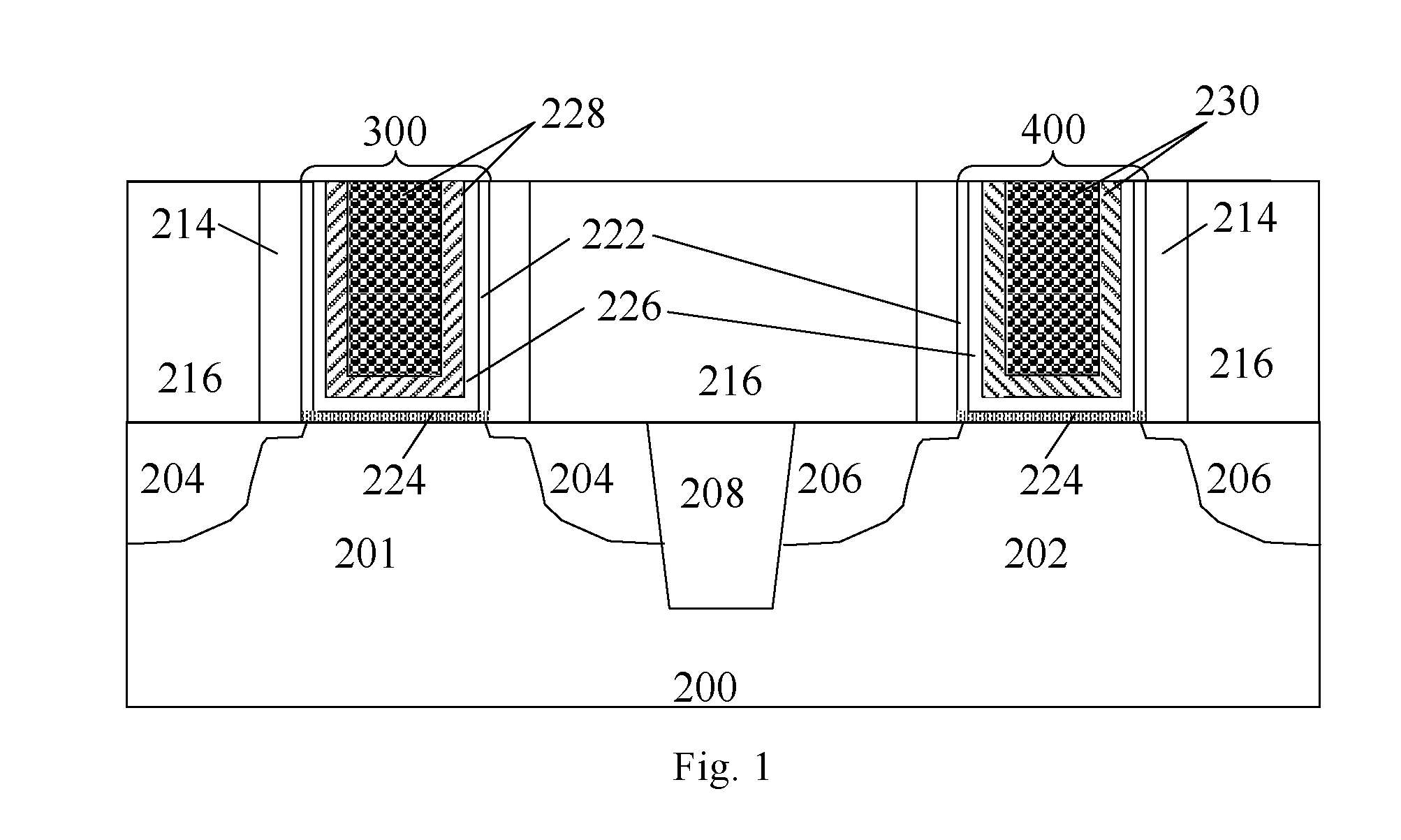
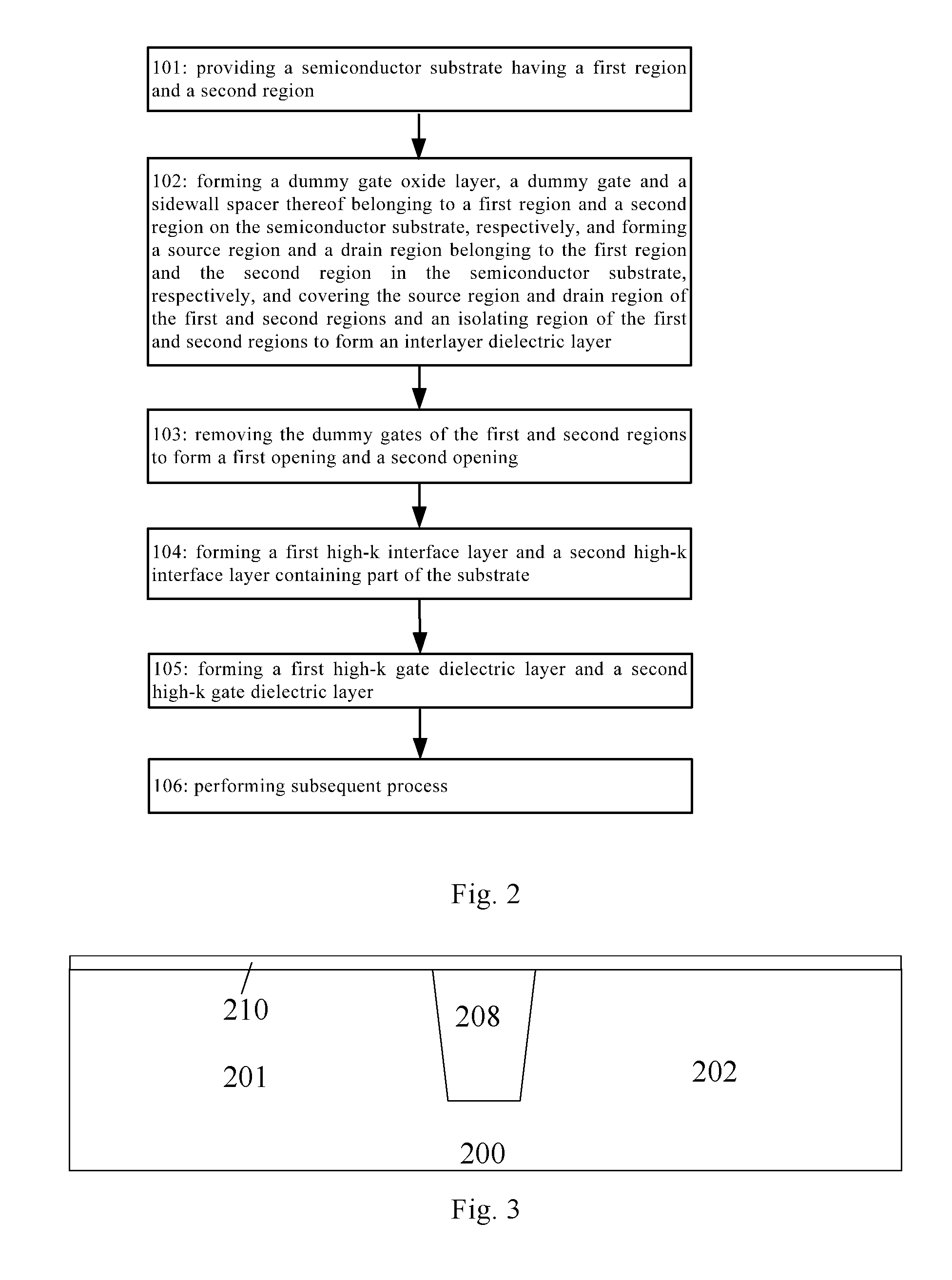
[0011]The present invention generally relates to a semiconductor device and a method of manufacturing the same, and more particularly, to a high-k gate dielectric / metal gate device with optimized interface based on the replacement gate process, and a method of manufacturing the same. The following disclosure provides a plurality of different embodiments or examples to achieve different structures of the present invention. To simplify the disclosure of the present invention, description of the components and arrangements of specific examples is given below. Of course, they are only illustrative and not intended to limit the present invention. Moreover, in the present invention, reference numbers and / or letters may be repeated in different embodiments. Such repetition is for the purposes of simplification and clearness, and does not denote the relationship between respective embodiments and / or arrangements being discussed. In addition, the present invention provides various examples f...


PUM

PropertyMeasurementUnit
thicknessaaaaaaaaaa
thicknessaaaaaaaaaa
thicknessaaaaaaaaaa

Abstract

A semiconductor device and a method of manufacturing the same are provided. A multi-component high-k interface layer containing elements of the substrate is formed from a ultra-thin high-k dielectric material in a single-layer structure of atoms by rapid annealing in the manufacturing of a CMOS transistor by the replacement gate process, and a high-k gate dielectric layer with a higher dielectric constant and a metal gate layer are formed thereon. The EOT of the device is effectively decreased, and the diffusion of atoms in the high-k gate dielectric layer from an upper level thereof is effectively prevented by the optimized high-k interface layer at high-temperature treatment. Thus, the present invention may also avoid the growth of the interface layers and the degradation of carrier mobility. Furthermore, the present invention may further alleviate the problem of high interface state and interface roughness caused by direct contact of the high-k gate dielectric layer with high dielectric constant and the substrate, and thus the overall performance of the device is effectively enhanced.

Description

FIELD OF THE INVENTION[0001]The present invention relates to a semiconductor device and a method of manufacturing the same, and more specifically, to a high-k gate dielectric / metal gate device with optimized interface based on a replacement gate process, and a method of manufacturing the same.BACKGROUND OF THE INVENTION[0002]With the development of the semiconductor industry, integrated circuits with higher performance and more powerful functions require greater element density. Thus, the sizes of the components need to be scaled further. The utilization of the core technology for 22 nanometers and beyond technology of integrated circuits has been the inevitable trend for the development of integrated circuits, which are also the projects for major international semiconductor companies and institutions to compete to develop. Study on CMOS device gate engineering with “high-k / metal gate” as the core technology is the most representative in 32 / 22 nanometer technology, and relevant stu...

Claims


Application Information

Patent Timeline
Patent Type & Authority Applications(United States)
IPC IPC(8): H01L27/088H01L21/28B82Y40/00B82Y99/00
CPCH01L21/823857Y10S438/926H01L29/66545
Inventor WANG, WENWUHAN, KAICHEN, SHIJIEWANG, XIAOLEICHEN, DAPENG
Owner INST OF MICROELECTRONICS CHINESE ACAD OF SCI
Why Eureka
Try Eureka