Reflective touch display panel and manufacturing method thereof

a display panel and touch technology, applied in the field of touch display panels, can solve the problems of reducing the sensitivity of the sensor in the integrated touch electronic paper display device, increasing the overall cost of the display device, and increasing the complexity of the manufacturing process, so as to reduce the sensitivity of the light sensing devi

Inactive Publication Date: 2011-10-20
AU OPTRONICS CORP
View PDF6 Cites 12 Cited by
  • Summary
  • Abstract
  • Description
  • Claims
  • Application Information

AI Technical Summary

Benefits of technology

[0008]A reflective touch display panel and a manufacturing method thereof are provided to solve the issue of lowering the sensitivity of the light sensing device.

Problems solved by technology

This technique increases not only the overall cost of the display device: but also the complexity of the manufacturing process.
In this case, the light sensor suffers from the problem of insufficient intensity of light, and the sensitivity of the sensor in the integrated touch electronic paper display device is lowered.. Therefore, the utility of touch operation is limited, and the quality of the product is affected accordingly.

Method used


Image

  • Reflective touch display panel and manufacturing method thereof
  • Reflective touch display panel and manufacturing method thereof
  • Reflective touch display panel and manufacturing method thereof

Examples


Embodiment Construction

[0026]Reference will now be made in detail to the present embodiments of the invention, examples of which are illustrated in the accompanying drawings. Wherever possible, the same reference numbers are used in the drawings and the description to refer to the same or like parts.

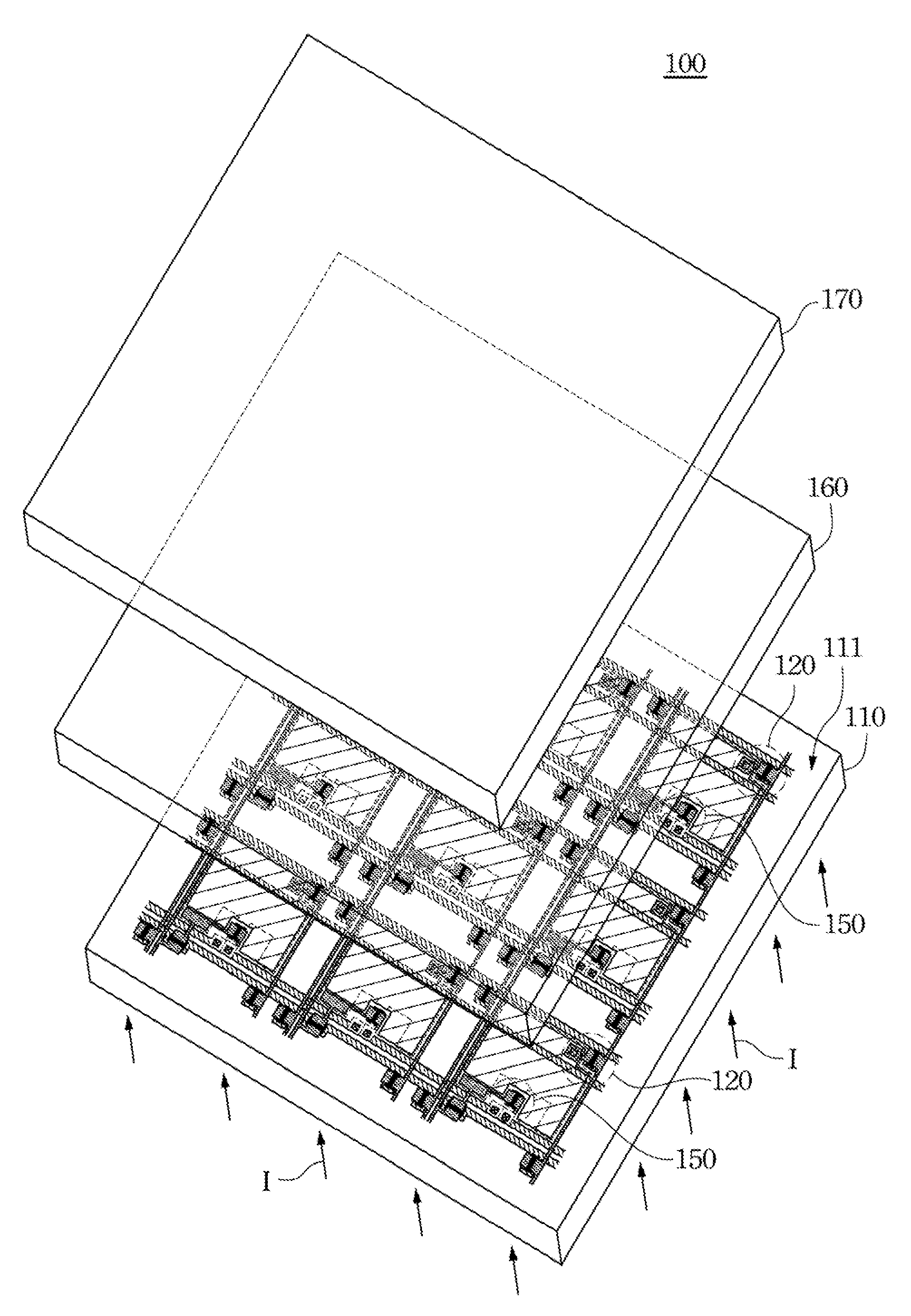
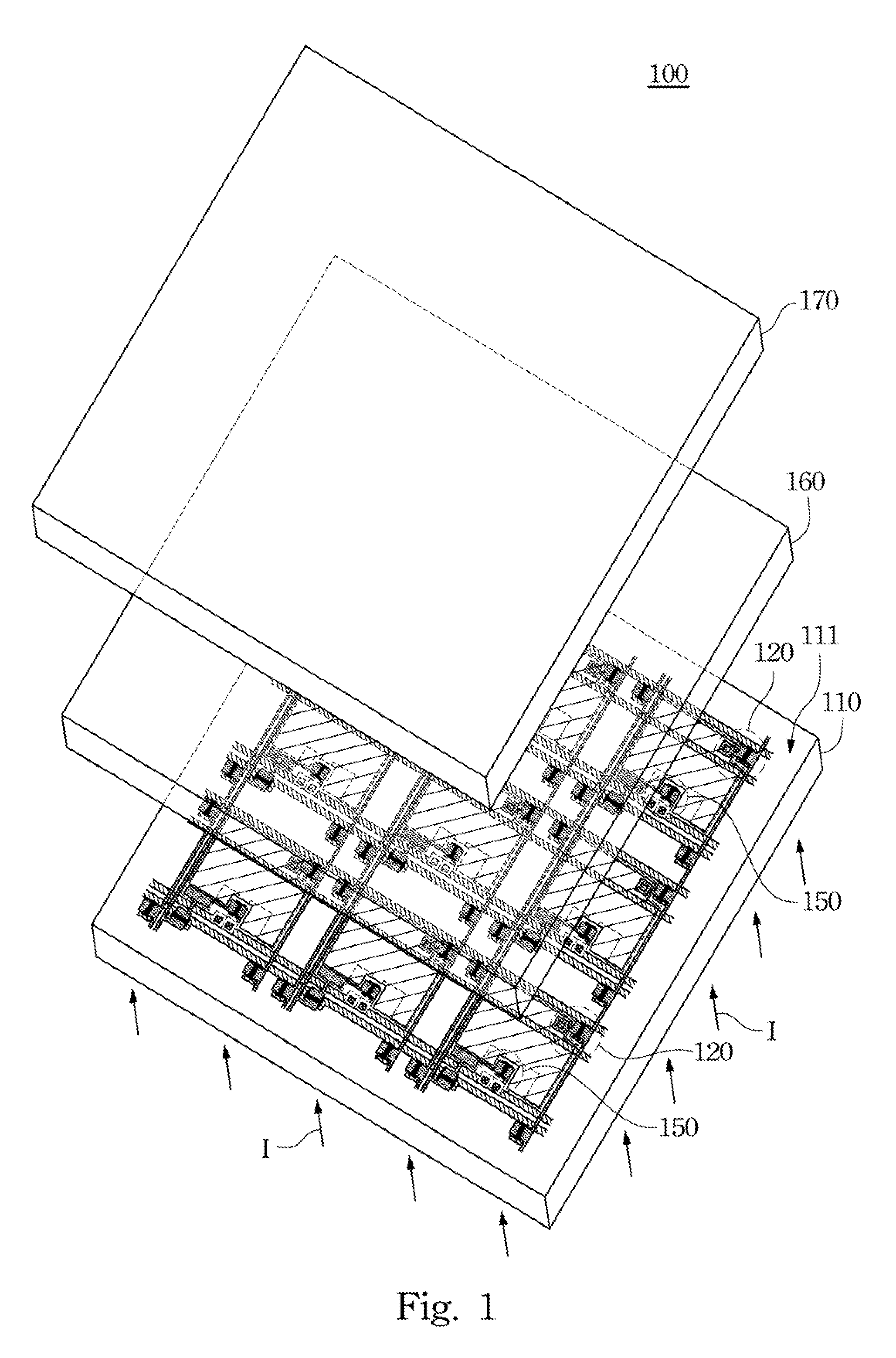
[0027]In the reflective touch display panel and the manufacturing method thereof, the light sensing device is disposed on the front substrate, and the light enters the display panel from the front substrate. Thus the light directly reaches the light sensing device, without passing through the reflective material layer first. The sensitivity of the light sensing device is increased and the product quality is improved.

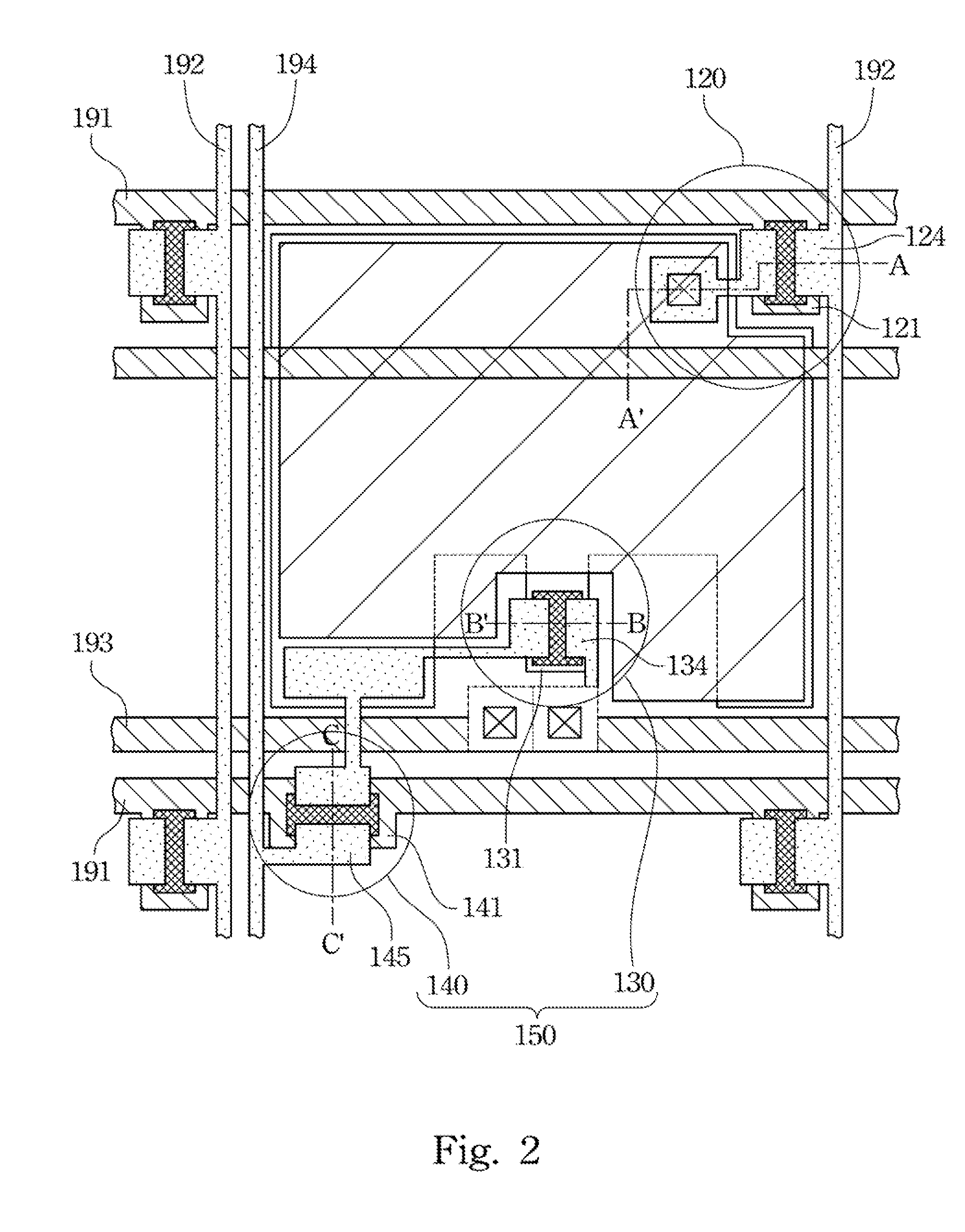
[0028]First, the detail description directs to a reflective touch display panel according to one embodiment of the invention. FIG. 1 is an exploded diagram of a reflective touch display panel according to one embodiment of the invention. The reflective touch display panel 100 includes a front subst...


PUM

PropertyMeasurementUnit
transparentaaaaaaaaaa
voltageaaaaaaaaaa
reflection rateaaaaaaaaaa

Abstract

A reflective touch display panel and a manufacturing method thereof are provided. An incident light enters the display panel through a front substrate thereof. A plurality of pixel structures and a plurality of light sensing devices are disposed on an inner surface of the front substrate. The light sensing device includes a light sensing transistor having a transparent gate electrode. The manufacturing method for the reflective touch display panel includes the following steps. A first patterned transparent conductive layer, including the transparent gate electrode and a capacitance lower electrode, is formed on the front substrate. A first patterned conductive layer, a dielectric layer, a patterned semi-conductive layer, a second patterned conductive layer and a second patterned transparent conductive layer are sequentially formed on the front substrate to respectively form the light sensing device and the pixel structure. A reflective material layer and a back substrate are. assembled on the front substrate to complete the reflective touch display panel.

Description

RELATED APPLICATIONS[0001]This application claims priority to Taiwan Application Serial Number 99112375, filed Apr. 20, 2010, which is herein incorporated by reference.BACKGROUND[0002]1. Technical Field[0003]The present invention relates to a touch display panel and a manufacturing method thereof. More particularly, the present invention relates to a reflective touch display panel and a manufacturing method thereof.[0004]2. Description of Related Art[0005]Along with the advances of manufacturing techniques for display devices, earlier heavy weight and high power consumption cathode ray tube display devices have been replaced with modern thin display devices. The thin display devices are now the main stream and the first priority option for consumers. In recent years, the energy issues are brought forth frequently, and the market made a higher standard for power consumption of display devices. In response to the requirement for greener display devices on the market, the industry has ...

Claims


Application Information

Patent Timeline
Patent Type & Authority Applications(United States)
IPC IPC(8): G06F3/042H01L31/18H01L33/00G02F1/167
CPCG02F1/167G06F3/0412G06F3/042H01L27/14687H01L31/113H01L27/14632H01L27/14678G06F2203/04103
Inventor LIN, HSIANG-LINHU, CHIH-JENHUANG, WEI-MING
Owner AU OPTRONICS CORP
Why Eureka
Try Eureka