Method for polishing silicon wafer, method for producing silicon wafer, apparatus for polishing disk-shaped workpiece, and silicon wafer

a technology of silicon wafers and polishing methods, applied in the direction of lapping machines, manufacturing tools, transportation and packaging, etc., to achieve the effect of not reducing the resistivity of the epitaxial layer, reducing the amount of spherical particles generated in the processing of wafers, and reducing the amount of spherical particles

Inactive Publication Date: 2011-10-20
SHIN-ETSU HANDOTAI CO LTD
View PDF5 Cites 8 Cited by
  • Summary
  • Abstract
  • Description
  • Claims
  • Application Information

AI Technical Summary

Benefits of technology

[0012]To achieve the above-mentioned object, according to the present invention, there is provided a method for polishing a silicon wafer, in which an oxide film is formed on a back surface side of the wafer, wherein at least, the oxide film on a chamfered portion of the silicon wafer is removed, and the oxide film on a peripheral portion of the back surface of the wafer is polished over at least 2 mm from the outermost peripheral portion of the back surface of the wafer so that a thickness of the polished oxide film decreases from inside to outside of the wafer.
[0037]Further, in the silicon wafer according to the present invention, particle generation caused in wafer handling can be remarkably reduced without the flatness of the peripheral portion of the wafer lowered, so that it becomes possible that particles do not attach to the wafer surface. Moreover, in the silicon wafer according to the present invention, it becomes possible that decrease of resistivity due to autodoping during epitaxial growth is not brought about.

Problems solved by technology

Furthermore, because the oxide film is not completely removed through polishing, it becomes possible that the back surface of the wafer is not exposed, and autodoping during epitaxial growth is not brought about.

Method used


Image

  • Method for polishing silicon wafer, method for producing silicon wafer, apparatus for polishing disk-shaped workpiece, and silicon wafer
  • Method for polishing silicon wafer, method for producing silicon wafer, apparatus for polishing disk-shaped workpiece, and silicon wafer
  • Method for polishing silicon wafer, method for producing silicon wafer, apparatus for polishing disk-shaped workpiece, and silicon wafer

Examples


example 1

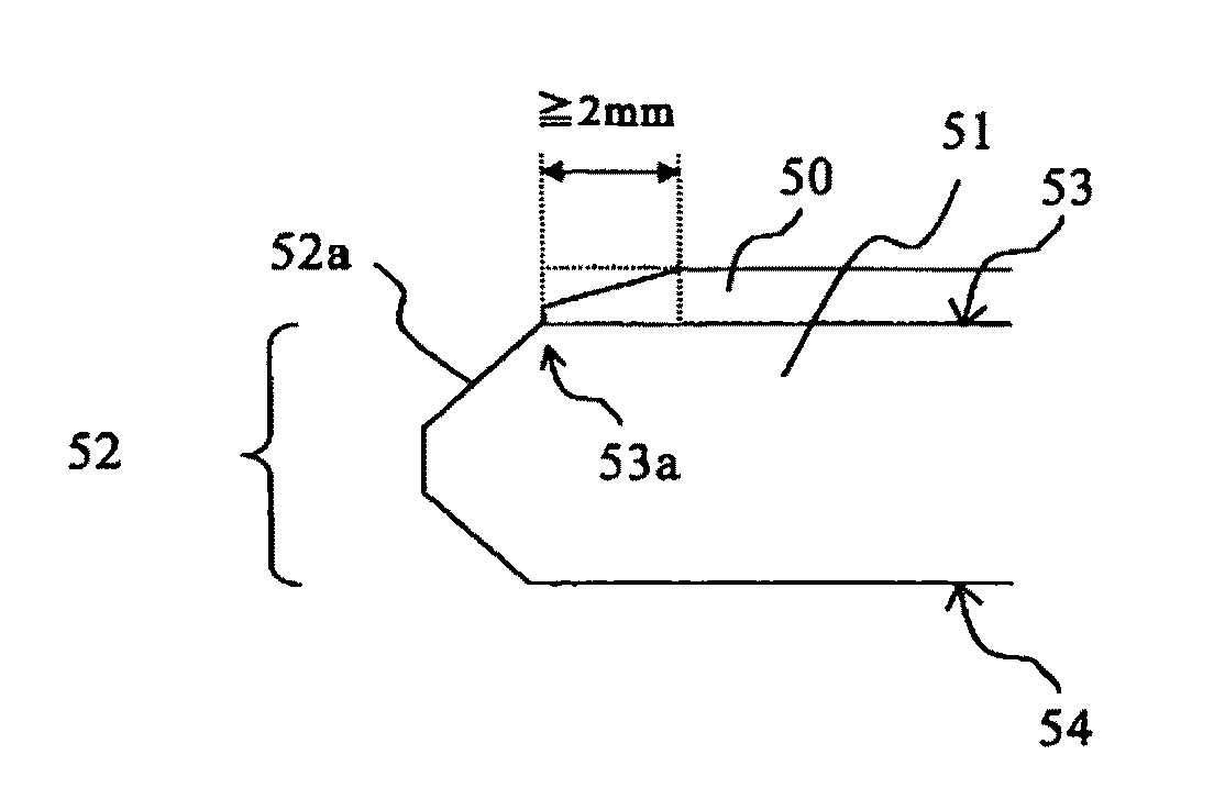
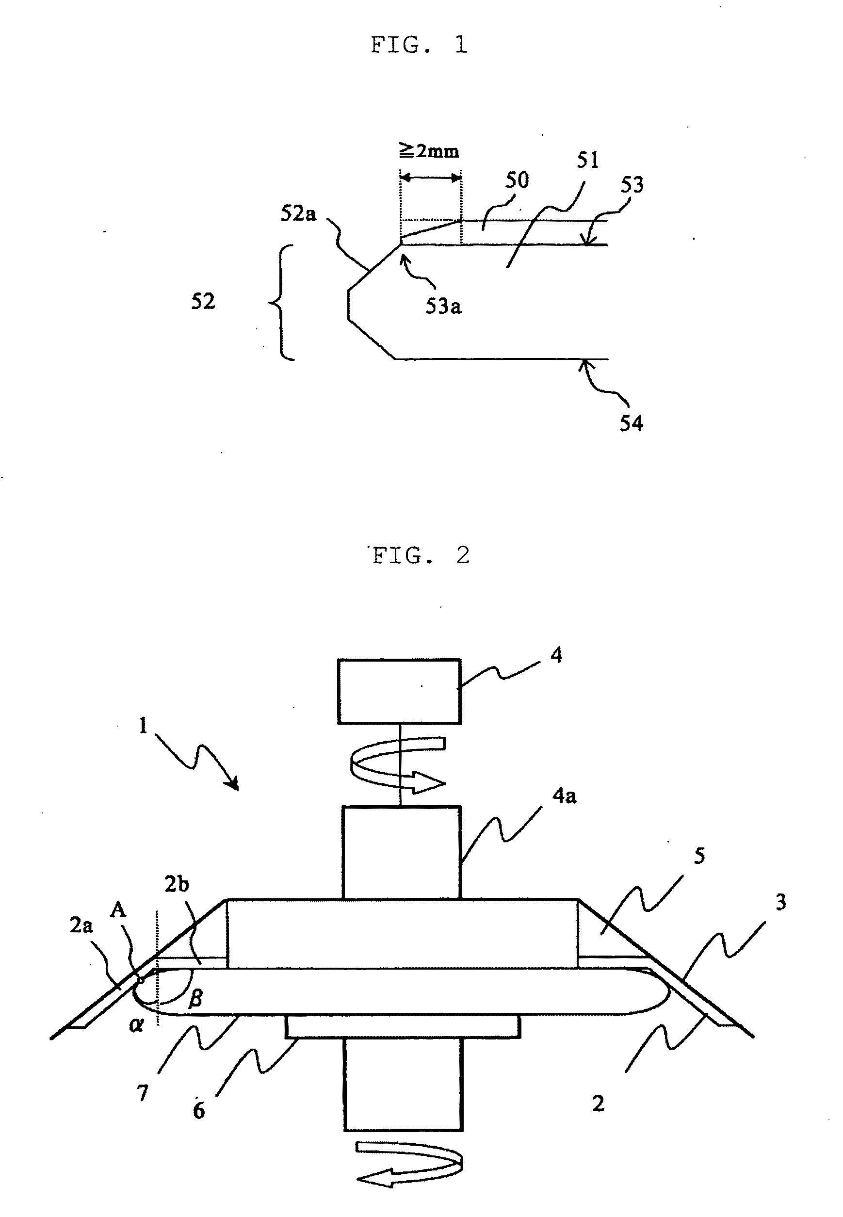
[0070]A silicon wafer (P type 0.01 Ω·cm: ) with a diameter of 300 mm produced by Czochralski method in which an oxide film was formed on a back surface and a chamfered portion was prepared, and the oxide film (thickness: 350 nm) on a peripheral portion of the back surface and the chamfered portion of the wafer was polished under the following conditions by using the polishing apparatus according to the present invention as shown in FIG. 2.

(Polishing Conditions)

[0071]Polishing pad: Suba400 (manufactured by Rodel, Inc.), ASKER C 61, thickness 1.27 mm)[0072]Angle with regard to polishing pad α: 70°, β: 90°[0073]Polishing pressure: 18 kgf[0074]Polishing agent: EDGE MIRROR V (manufactured by Fujimi Incorporated)[0075]Rotating rate of rotating body: 600 rpm[0076]Polishing time: 45 sec

[0077]The peripheral portion of the back surface and the chamfered portion of the back surface side were polished under the above-described conditions, subsequently the wafer was sucked to a holder with the f...

examples 2 and 3

[0078]Polishing was performed under the same conditions as Example 1, except that each polishing pressure was set at 12 kgf (Example 2), 6 kgf (Example 3), and each polishing time was set at 30 sec (Example 2) and 20 sec (Example 3).

examples 4-5

, Comparative Examples 4-6

[0096]Next, in order to confirm the effects of the polishing apparatus according to the present invention, polishing was performed with the angles α and β with regard to the polishing pad changed as follows. The polishing conditions were the same as Example 1 except for the angles.

Comparative example 4 α: 30°, β: 90°Example 4α: 40°, β: 90°Comparative example 5α: 80°, β: 90°Comparative example 6α: 70°, β: 120°Example 5α: 70°, β: 110°

[0097]Each wafer polished under the above-described conditions was transferred with a robot transfer device for five times, then the thickness of the oxide films on the chamfered portions and the peripheral portions of the back surfaces was measured with film thickness measuring device of interference fringe type (TFM120). Further, the number of particles on each wafer surface was measured with a particle counter (LS6500). The results are shown in Table 1.

TABLE 1Measurementresults ofthe numbersMeasurement results of oxide filmsof...


PUM

PropertyMeasurementUnit
angleaaaaaaaaaa
angleaaaaaaaaaa
thicknessaaaaaaaaaa

Abstract

The present invention is a method for polishing a silicon wafer, in which an oxide film is formed on a back surface side of the wafer, wherein the oxide film on a chamfered portion of the silicon wafer is removed, and the oxide film on a peripheral portion of the back surface of the wafer is polished over at least 2 mm from the outermost peripheral portion of the back surface of the wafer so that a thickness of the polished oxide film decreases from inside to outside of the wafer, a method for producing such a silicon wafer, and a silicon wafer. Thereby, there are provided a method for polishing a silicon wafer in which particles' attaching to a wafer surface after handling can be prevented, decrease of resistivity due to autodoping is not brought about, and moreover, productivity does not decrease; a method for producing such a silicon wafer; an apparatus for polishing a disk-shaped workpiece suitable for performing the methods; and a silicon wafer in which particles do not attach to a surface after handling even if an oxide film is formed on a back surface of the wafer and decrease of resistivity due to autodoping is not brought about.

Description

[0001]This is a Division of application Ser. No. 11 / 794,126 filed Jun. 26, 2007, which in turn is a National Phase of PCT / JP2005 / 023024, which claims the benefit of Japanese Application No. 2004-379526 filed Dec. 28, 2004. The disclosure of the prior applications are hereby incorporated by reference herein in their entirety.TECHNICAL FIELD[0002]The present invention relates to a method for polishing a silicon wafer, a method for producing a silicon wafer, an apparatus for polishing a disk-shaped workpiece, and a silicon wafer. To be more specific, the present invention relates to a method for polishing a silicon wafer in which an oxide film is formed on a back surface and a chamfered portion of the wafer, a method for producing such a silicon wafer, an apparatus for polishing a disk-shaped workpiece suitable for the polishing method, and a silicon wafer in which an oxide film is formed on a back surface of the wafer.BACKGROUND ART[0003]When a thin film is formed on a front surface o...

Claims


Application Information

Patent Timeline
Patent Type & Authority Applications(United States)
IPC IPC(8): B24B7/10B24B37/02B24B37/20H01L21/304
CPCB24B9/065Y10T428/24488H01L21/02024H01L21/02021H01L21/304
Inventor MIZUSHIMA, KAZUTOSHI
Owner SHIN-ETSU HANDOTAI CO LTD
Why Eureka
Try Eureka