Ac-plasma display devices using metal nanoparticles or nanostructures and method for manufacturing the same

a technology of ac plasma display device and nanostructure, which is applied in the manufacture of electrode systems, electric discharge tubes/lamps, and discharge tubes luminescnet screens, etc., can solve the problems of difficult to reduce the consumption of power, the luminescent efficiency of phosphor produced through such attempts is not actually greater than that of commonly used phosphors, etc., to improve the luminescent characteristics of phosphors, reduce the manufacturing cost of ac plasma display devices, and improve the luminescent characteristics of phospho

Inactive Publication Date: 2011-10-27
KOREA ADVANCED INST OF SCI & TECH
View PDF2 Cites 9 Cited by
  • Summary
  • Abstract
  • Description
  • Claims
  • Application Information

AI Technical Summary

Benefits of technology

[0041]According to the present invention, since the luminescent characteristics of a phosphor can be improved using irregularly-arranged metal nanoparticles or regularly-arranged metal nanostructures, the brightness of an AC plasma display device, such as an AC plasma lamp, an AC plasma display panel or the like, can be improved.
[0042]That is, according to the present invention, a surface plasmon resonance phenomenon can be induced using metal nanoparticles or metal nanostructures without changing the composition of a phosphor to improve the luminescent characteristics of the phosphor, so that the manufacturing cost of an AC plasma display device can be decreased and the luminescent efficient thereof can be improved, with the result that the power consumption of the AC plasma display device can be decreased and the brightness thereof can be improved, thereby improving the efficiency of the AC plasma display device.
[0043]Further, according to the present invention, since a metal nanoparticle layer composed of Ag, Au, Cu, Al or the like is additionally formed on a protective film of a front panel, the secondary electron emission rate of an AC plasma display device can be increased by the surface plasmon excitation induced around the metal nanoparticles under the influence of photons, such as vacuum ultraviolet (VUV), infrared (IR), visible ray or the like, generated from discharge cells, so that the driving voltage of the AC plasma display device can be decreased and the discharge efficiency thereof can be improved.
[0044]That is, according to the present invention, when photons are incident on a protective film (MgO) including metal nanoparticles, the excitation of electrons is accelerated by the strong local field generated around the metal nanoparticles, thus increasing the secondary electron emission coefficient of the protective film (MgO), so that the secondary electron emission coefficient in discharge cells is also increased, with the result that the driving voltage of the AC plasma display device is decreased and the discharge efficiency thereof is improved, thereby realizing a high-efficiency AC plasma display panel.
[0045]Furthermore, according to the present invention, a metal nanoparticle layer formed in a protective film functions to optically absorb the neon (Ne) and infrared (IR) generated at the time of plasma discharge and thus to store the energy generated from the plasma discharge in metal nanoparticles and to increase the temperature of the region adjacent to the nanoparticle layer, so that the secondary electron emission coefficient and exo-electron emission rate of the AC plasma display device are increased, with the result that the address delay time thereof is decreased, thereby realizing a high-resolution AC plasma display panel.

Problems solved by technology

However, the luminescent efficiency of the phosphors produced through such attempts is not actually greater than that of commonly-used phosphors.
However, since these technologies do not increase the emission rate of secondary electrons to the MgO-doped protective film, they are problematic in that it is difficult to reduce the consumption of power by decreasing discharge voltage and increasing luminescent efficiency.

Method used


Image

  • Ac-plasma display devices using metal nanoparticles or nanostructures and method for manufacturing the same
  • Ac-plasma display devices using metal nanoparticles or nanostructures and method for manufacturing the same
  • Ac-plasma display devices using metal nanoparticles or nanostructures and method for manufacturing the same

Examples


Embodiment Construction

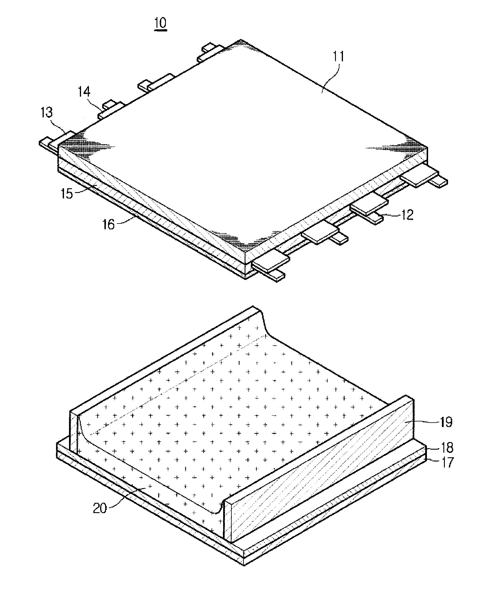
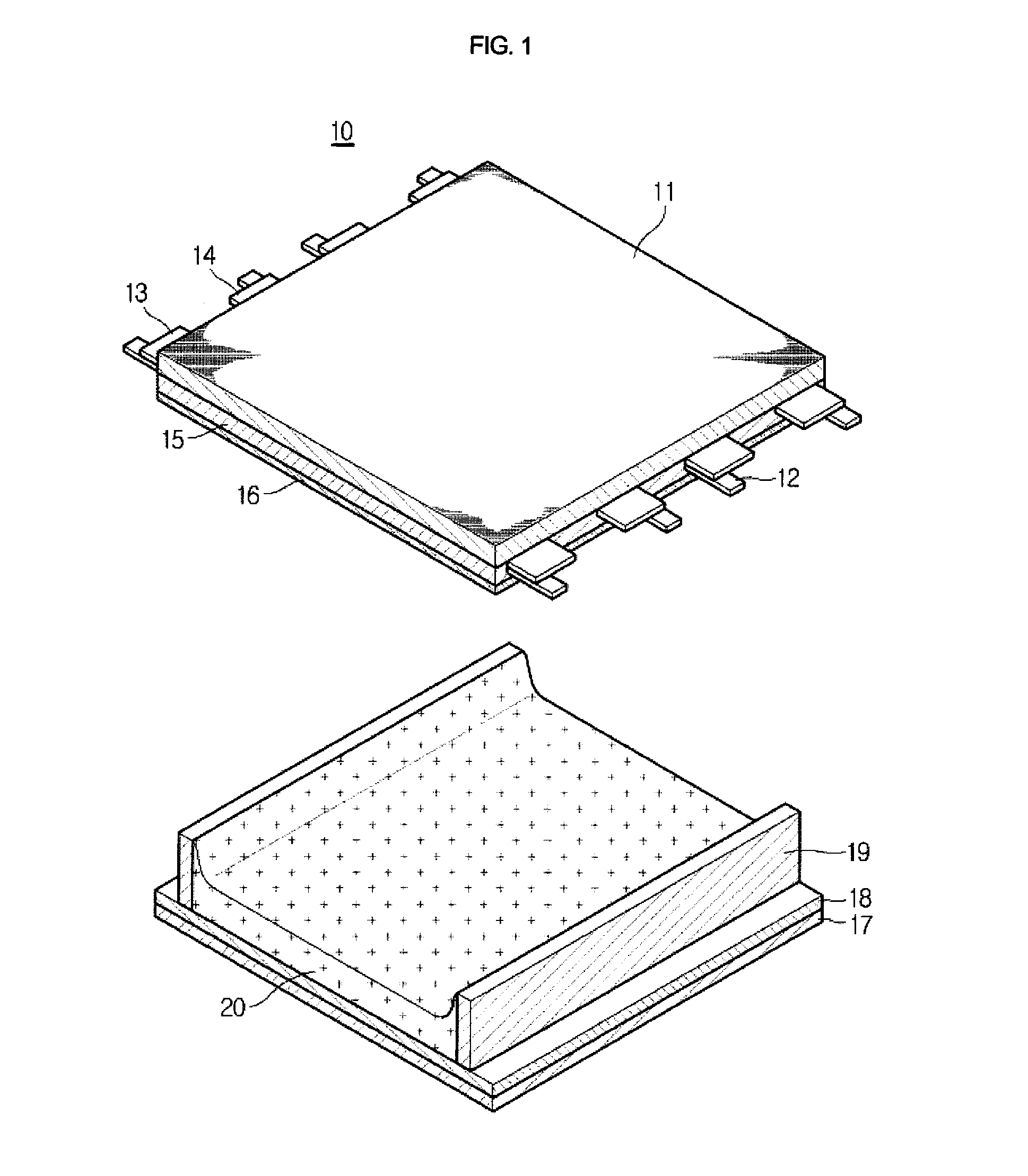
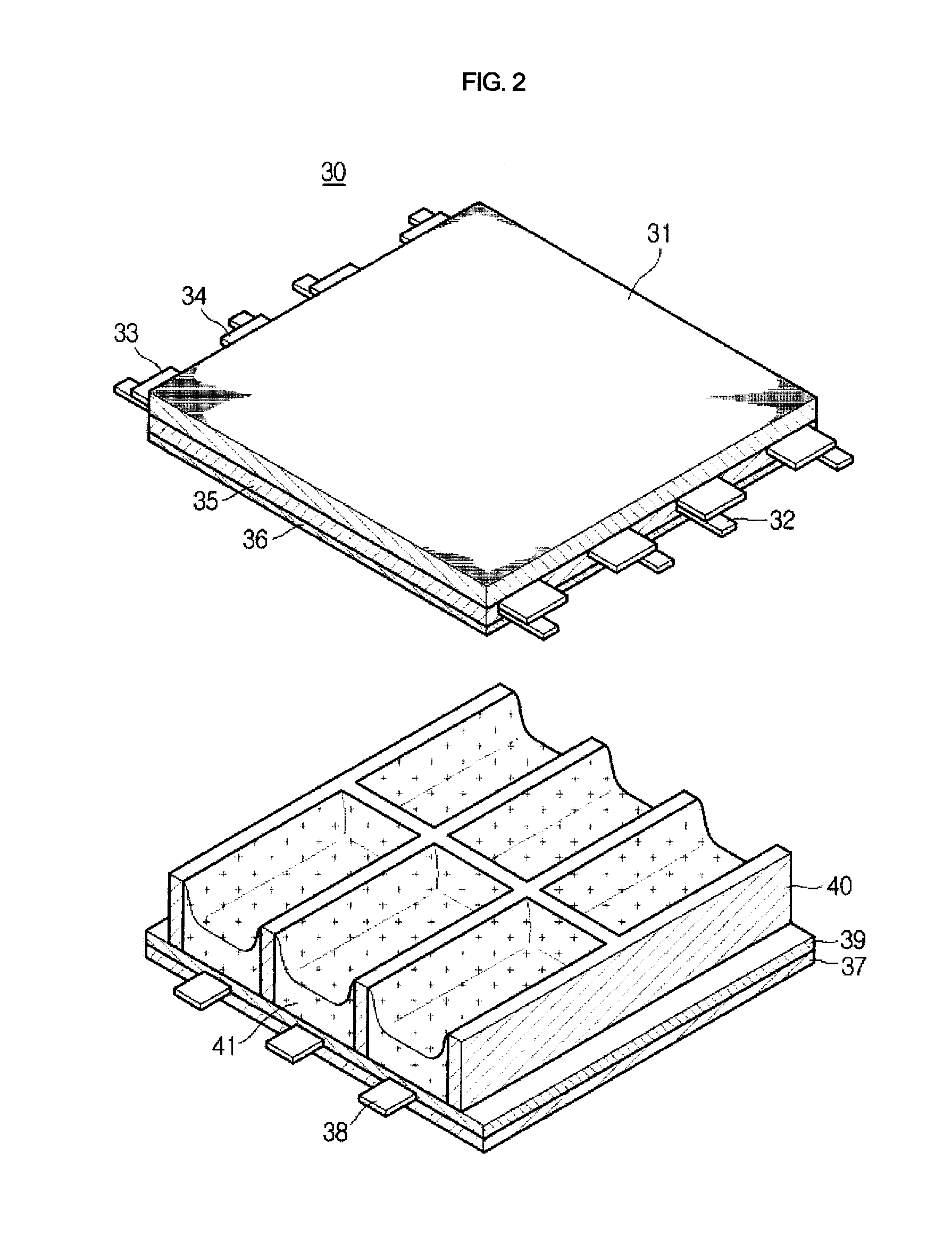
[0060]Hereinafter, preferred embodiments of the present invention will be described in detail with reference to the attached drawings.

[0061]An AC plasma display panel including a phosphor layer provided with metal nanostructures will be described with reference to FIGS. 3 to 13, and an AC plasma display panel including a protective film provided with metal nanostructures will be described with reference to FIGS. 14 to 18. Further, an AC plasma display panel in which both a phosphor layer and a protective film are provided with metal nanoparticles will be described with reference to FIG. 19.

[0062]For reference, in the present invention, metal nanostructures may include metal nanoparticles, metal nanotubes, metal nanorods, metal nanowires and the like. The detailed description thereof is as follows.

[0063]First, an AC plasma display panel including a phosphor layer provided with metal nanostructures will be described with reference to FIGS. 3 to 13.

[0064]FIG. 3 is a perspective view sh...


PUM


Abstract

The present invention provides an AC plasma display device using metal nanostructures, including: a front panel and a rear panel which are disposed in parallel to each other and at least one of which is provided with electrodes for gas discharge; an electrode layer, a front dielectric layer and a protective film which are sequentially formed on a side of the front panel which faces the rear panel; a phosphor layer which is formed on the rear panel and which is excited and simultaneously radiated by gas discharge occurring in the electrodes; and metal nanostructures included in the protective film and the phosphor layer, and provides a method of manufacturing the same. The AC plasma display device can improve a secondary electron emission coefficient and photoluminescent intensity using surface plasmon excitation because it is provided with a protective film including metal nanostructures.

Description

BACKGROUND OF THE INVENTION[0001]1. Field of the Invention[0002]The present invention relates to an AC plasma display device, such as an AC plasma lamp, an AC plasma display panel or the like, using plasma discharge, and a method of manufacturing the same.[0003]2. Description of the Related Art[0004]An AC plasma lamp or an AC plasma display panel (hereinafter, referred to as an “AC PDP”) displays an image because vacuum ultraviolet rays having a wavelength of 140˜180 nm, which are generated when an inert gas mixture, such as He+Xe, Ne+Xe or the like, is discharged in partitioned discharge cells, cause a phosphor to emit light.[0005]FIGS. 1 and 2 are perspective views showing general AC plasma display devices, wherein FIG. 1 shows a flat AC plasma lamp 10, and FIG. 2 shows a flat AC plasma display panel 30. Though these display devices have in common the fact that they are display devices using plasma discharge, they differ from each other in structural aspect.[0006]As shown in FIG. ...

Claims


Application Information

Patent Timeline
Patent Type & Authority Applications(United States)
IPC IPC(8): H01J63/04H01J9/24H01J11/12H01J11/40H01J11/42
CPCH01J9/02H01J11/42H01J11/40H01J11/12
Inventor LEE, SEONG MINCHO, KWAN HYNNKIM, WOO HYUNYANG, KI YOULCHOI, KYUNG CHEOL
Owner KOREA ADVANCED INST OF SCI & TECH
Why Eureka
Try Eureka