Bandgap reference circuit and method

a reference circuit and band gap technology, applied in the field of band gap reference voltage circuits, can solve the problems of reducing the value of vsub>be /sub>voltage, wide chip-to-chip variation, and poor long-term stability of conventional band gap reference circuits such as the one in prior art fig. 1a, so as to reduce random chip-to-chip variation in a band gap reference voltage

Active Publication Date: 2011-10-27
TEXAS INSTR INC
View PDF7 Cites 10 Cited by
  • Summary
  • Abstract
  • Description
  • Claims
  • Application Information

AI Technical Summary

Benefits of technology

[0020]It is an object of the invention to provide a band gap reference voltage circuit and method that substantially reduces random chip-to-chip variation in a band gap reference voltage generated thereby.

Problems solved by technology

Conventional band gap reference circuits such as the one in Prior Art FIG. 1A generally have a serious problem of poor long term stability and wide chip-to-chip variation in the thermal drift of the generated reference voltage VREF.
Bandgap reference circuit 1 is difficult to optimize, because although reduction of the ratio of the emitter areas and emitter current densities of transistors Q4 and Q5 leads to better component matching, such reduction also reduces the value of the ΔVBE voltage, so higher amplifier gain is required.
That unfortunately results in higher variation of the generated reference voltage VREF due to the “gained-up” input offset voltage and associated drift of the offset voltage of amplifier 4, and hence results in higher noise in the generated reference voltage VREF.
The problem arises that, in order to generate the ΔVBE voltage, it is necessary to use both a large-area transistor and a small-area transistor.
But the random variation depends not much on the large-area transistor Q4 but mainly on the single small-area unit transistor Q5, and consequently there is no way to optimally reduce the effect of the single small-area unit transistor.)
However, even though dynamic element matching techniques are widely used in many applications, such techniques nevertheless are unsuitable in many applications because dynamic element matching typically involves highly complex, very costly circuitry, slow circuit operation, and generation of ripple signals or tones which are very difficult and costly to deal with.

Method used


Image

  • Bandgap reference circuit and method
  • Bandgap reference circuit and method
  • Bandgap reference circuit and method

Examples


Embodiment Construction

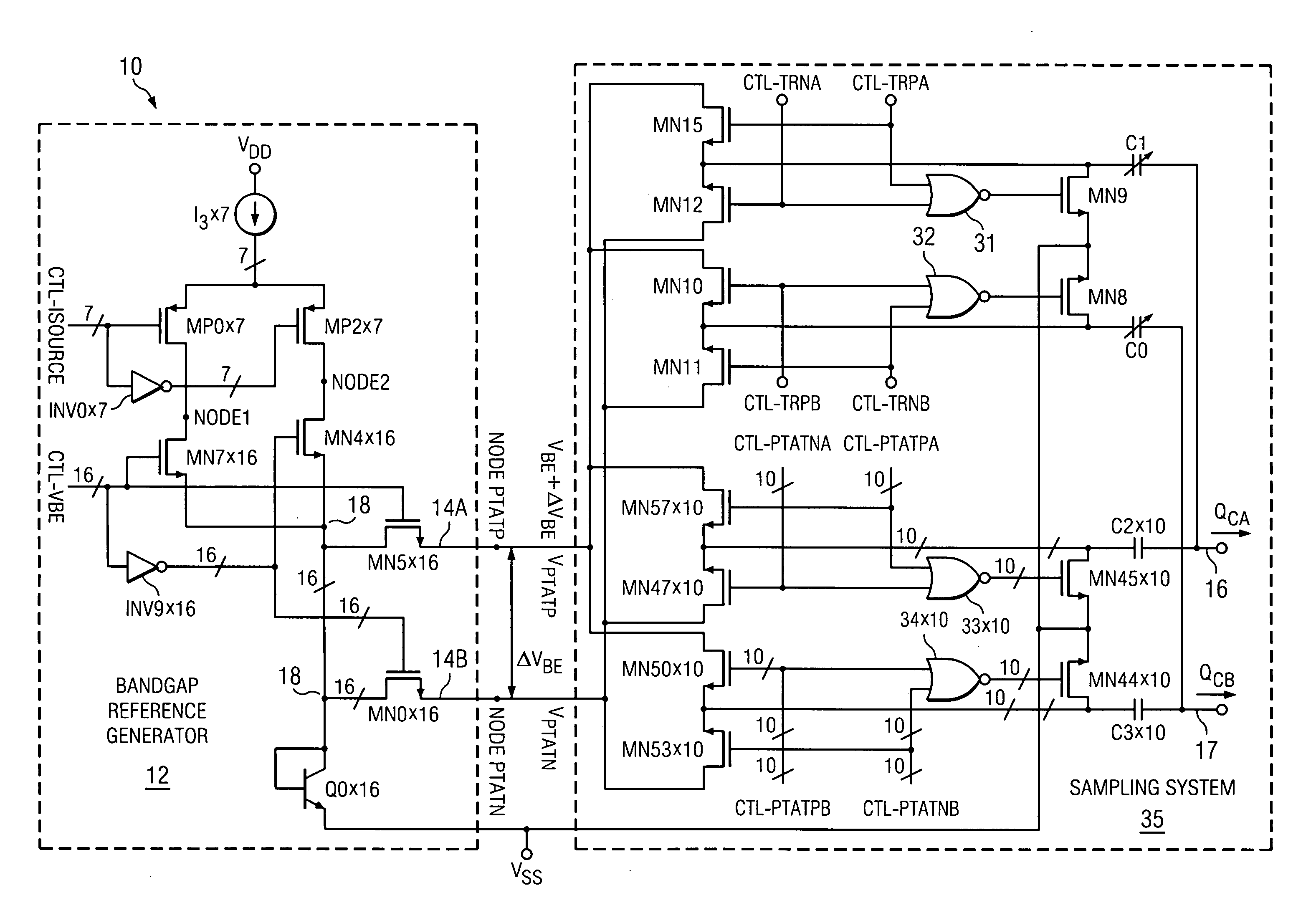
[0050]Structure of FIG. 2A, block 12

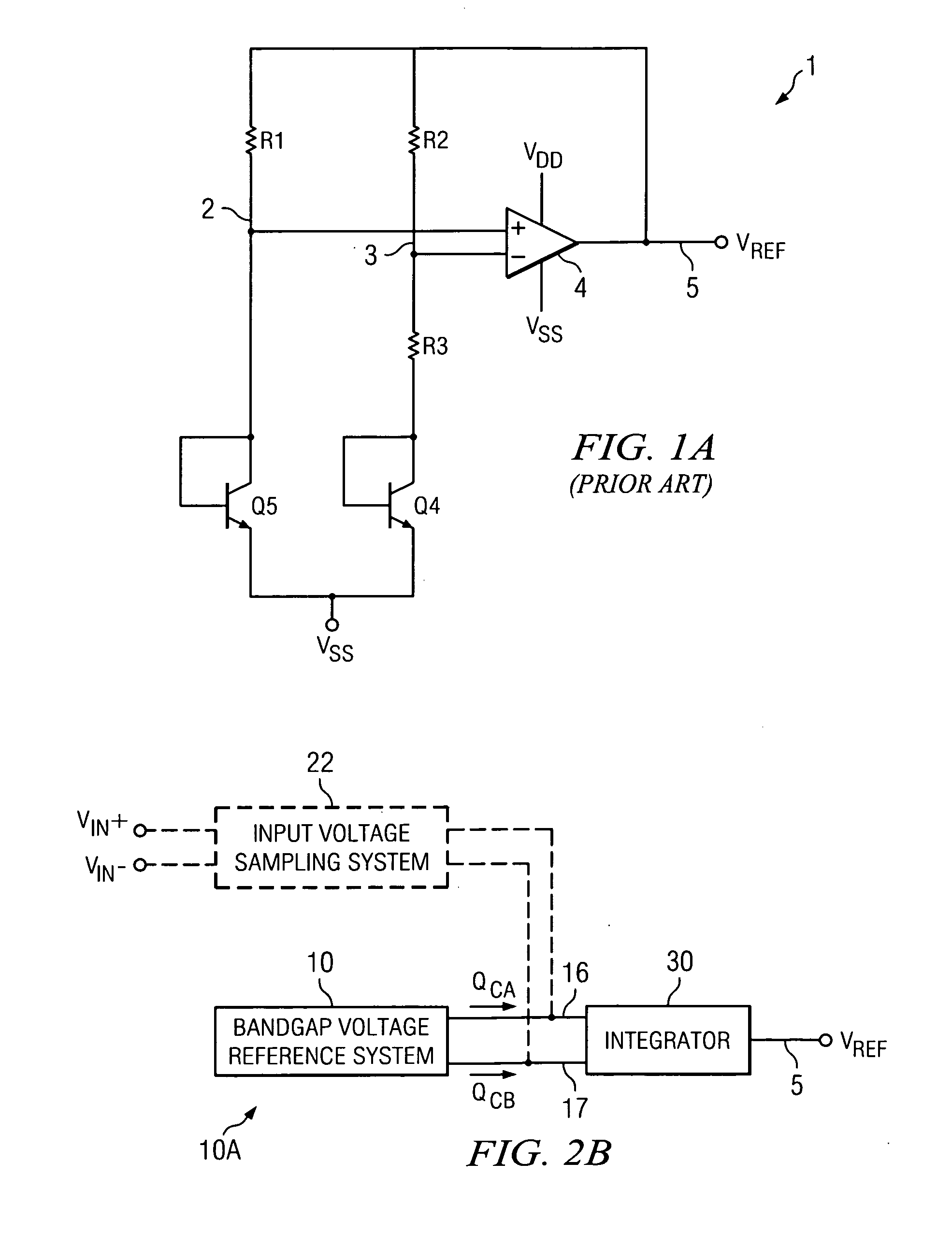
[0051]FIG. 2A shows a bandgap voltage reference system 10 with dynamic element matching to reduce circuit inaccuracy due to normal variations in parameters of various circuit components. Voltage reference system 10 includes a bandgap reference generator circuit 12, the output of which is coupled to a dynamic sampling system 35. In this example, reference generator circuit 12 includes M=7 identical current sources I3, collectively designated “I3×7”. Each of the 7 current sources I3 has one terminal connected to VDD and another terminal connected to the source of a corresponding P-channel transistor MP0 and also to the source of another corresponding P-channel transistor MP2. The 7 transistors MP0 are collectively designated “MP0×7”, and the 7 transistors MP2 are collectively designated “MP2×7”. The gates of transistors MP0×7 are connected to the 7 conductors, respectively, of a bus which conducts the M=7 bits of a digital control signal CTL-ISOURCE...


PUM


Abstract

A circuit for generating a band gap reference voltage (VREF) includes circuitry (I3×7) for supplying a first current to a first conductor (NODE1) and a second current to a second conductor (NODE2). The first conductor is successively coupled to a plurality of diodes (Q0×16), respectively, in response to a digital signal (CTL-VBE) to cause the first current to successively flow into selected diodes. The second conductor is coupled to collectors of the diodes which are not presently coupled to the first conductor. The diodes are successively coupled to the first conductor so that the first current causes the diodes, respectively, to produce relatively large VBE voltages on the first conductor and the second current causes sets of the diodes not coupled to the first conductor to produce relatively small VBE voltages on the second conductor. The relatively large and small VBE voltages provide differential band gap charges (QCA-QCB) which are averaged to provide a stable band gap reference voltage (VREF).

Description

BACKGROUND OF THE INVENTION[0001]The present invention relates generally to bandgap reference voltage circuits, and more particularly to improvements therein which would improve accuracy by reducing sensitivity to random mismatching of internal components and sensitivity to temperature, long-term drift of input offset voltages, and mechanical stresses in integrated circuit chips in which the bandgap reference voltage circuits are formed.[0002]FIG. 1A shows a conventional bandgap voltage reference circuit 1 which includes an amplifier 4 having its (+) input connected to the junction 2 between one terminal of a resistor R1 and the base and collector of a diode-connected NPN transistor Q5. Similarly, the (−) input of amplifier 4 is connected to the junction 3 between one terminal of a resistor R2 and one terminal of a resistor R3. The other terminal of resistor R3 is connected to the base and collector of a diode-connected NPN transistor Q4. The upper terminals of resistors R1 and R2 a...

Claims


Application Information

Patent Timeline
Patent Type & Authority Applications(United States)
IPC IPC(8): G05F3/16
CPCG05F3/30H03F2200/447H03F1/303
Inventor TRIFONOV, DIMITAR T.DOORENBOS, JERRY L.
Owner TEXAS INSTR INC
Why Eureka
Try Eureka