Thin film coating pinning arrangement

a thin film coating and arrangement technology, applied in the field of pining regions, can solve the problems of the most expensive component of the photovoltaic solar collection system, the photovoltaic cell, and achieve the effect of significantly reducing the likelihood of cracking or delamination

Inactive Publication Date: 2011-11-03
SKYLINE SOLAR INC
View PDF6 Cites 27 Cited by
  • Summary
  • Abstract
  • Description
  • Claims
  • Application Information

AI Technical Summary

Benefits of technology

[0004]The present invention relates to the use of pinning regions to strengthen the adhesive bond between different layers of an optical or electrical component such that the likelihood of cracking or delamination is significantly reduced.
[0005]In one aspect of the present invention, a photovoltaic cell for use in a solar collector is described. The photovoltaic cell includes two electrically conductive layers that are positioned on a surface of a semiconductor substrate. The first conductive layer is adhered to and in direct contact with a surface of the semiconductor substrate. The second conductive layer has a different composition from and is substantially more electrically conductive than the first conductive layer. There are multiple spaced apart pinning regions that are distributed through an interface between the first and second conductive layers. The pinning regions, help locally anchor the two layers. The adhesive strength of the pinning regions to the second conductive layer is greater than the adhesive strength of the first conductive layer to the second conductive layer.

Problems solved by technology

Typically, the most expensive component of a photovoltaic (PV) solar collection system is the photovoltaic cell.

Method used


Image

  • Thin film coating pinning arrangement
  • Thin film coating pinning arrangement
  • Thin film coating pinning arrangement

Examples


Embodiment Construction

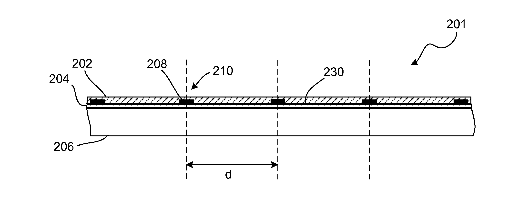
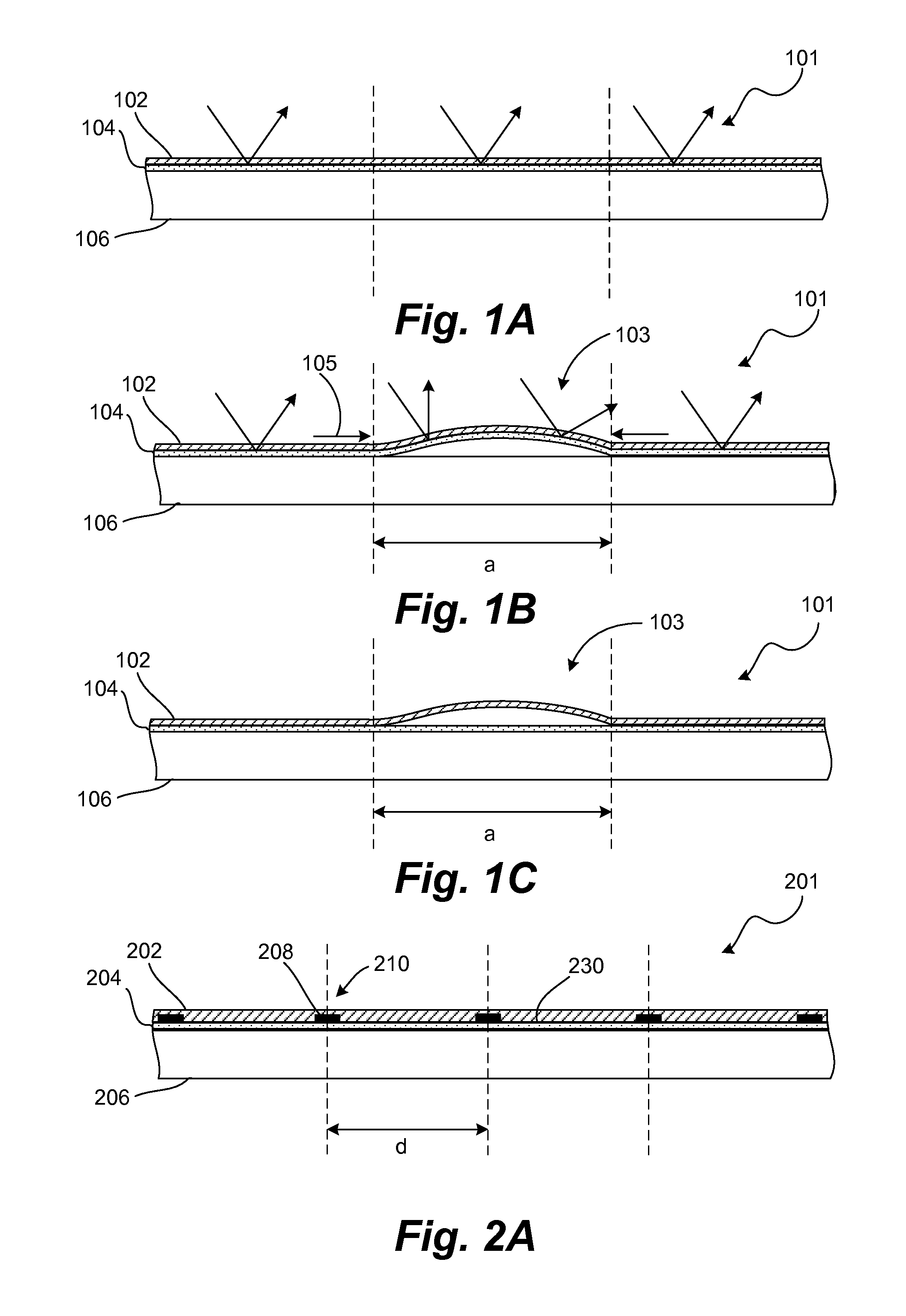
[0024]In some concentrating photovoltaic systems, a reflector is used to reflect incident light towards a solar receiver. Ideally, the reflector has a high quality optical surface. If the reflector surface is degraded, the incident light may be absorbed or scattered and never reach the solar receiver.

[0025]In operation, the reflector is exposed to the ambient environment and various environmental stresses, such as temperature fluctuation, ultraviolet light exposure, and moisture. These stresses can cause portions of the reflector to blister or crack. As a result, the light may be scattered or absorbed.

[0026]An example of this problem is diagrammatically illustrated in FIGS. 1A-1C. For purposes of comparison, FIG. 1A illustrates an example of an undamaged reflector 101. The reflector 101 includes a substrate 106, a reflective coating 104 and a protective layer 102. The protective layer 102, which is typically made of an optically transparent material, is formed over the other layers ...


PUM


Abstract

In one aspect of the present invention, a photovoltaic cell for use in a solar collector is described. The photovoltaic cell includes two electrically conductive layers that are positioned on a surface of a semiconductor substrate. The first conductive layer is adhered to and in direct contact with a surface of the semiconductor substrate. The second conductive layer has a different composition from and is substantially more electrically conductive than the first conductive layer. There are multiple spaced apart pinning regions that are distributed through an interface between the first and second conductive layers. The pinning regions, help locally anchor the two layers. Some aspects of the present invention relate to the use of pinning regions in other types of optical or electrical components.

Description

CROSS-REFERENCE TO RELATED APPLICATIONS[0001]This application claims priority to U.S. Provisional Patent Application No. 61 / 329,482, filed Apr. 29, 2010, entitled “Reflective Coating,” which is incorporated herein in its entirety for all purposes.FIELD OF THE INVENTION[0002]The present invention relates generally to the use of pinning regions to help adhere a thin film layer of an optical or electrical device to an adjacent layer or substrate. One particular application relates to the use of pinning regions in the reflector of a concentrating solar energy collector to help adhere a thin film reflective layer to a supporting surface. In other applications, similar pinning regions may be used in other types of optical or electrical components such as photovoltaic cells, mirrors, reflectors, windows, etc.BACKGROUND OF THE INVENTION[0003]Typically, the most expensive component of a photovoltaic (PV) solar collection system is the photovoltaic cell. To help conserve photovoltaic material...

Claims


Application Information

Patent Timeline
Patent Type & Authority Applications(United States)
IPC IPC(8): H01L31/0216H01L31/18H01L31/0232F24S23/79
CPCF24J2/16F24J2002/1071G02B7/008G02B7/181H01L31/02168Y10T428/24826G02B19/0019G02B19/0042G02B19/0023Y02E10/40H01L31/056Y02E10/52F24S2023/86F24S23/77Y10T428/249923
Inventor FINOT, MARC A.ACKLER, HAROLD D.
Owner SKYLINE SOLAR INC
Why Eureka
Try Eureka