Device and method for transient voltage suppressor

Active Publication Date: 2011-11-03
BCD SHANGHAI MICRO ELECTRONICS CO LTD
View PDF8 Cites 13 Cited by
  • Summary
  • Abstract
  • Description
  • Claims
  • Application Information

AI Technical Summary

Benefits of technology

[0006]As described above, certain conventional electrostatic discharge (ESD) protection devices employ a buried n+/p+ junction as a Zener diode, with other device fabricated on top of the Zener device. These Zener diode devices tend to have limitations. For example, the multiple thermal processing steps, such as epitaxial growth, diffusions, and oxidations, tend to cause the p+ dopants from the substrate to out diffuse.

Problems solved by technology

These Zener diode devices tend to have limitations.
The resultant graded doping profile at the Zener junction can often result in higher than desired Zener breakdown voltages and make it difficult to accurately control the associated cla

Method used


Image

  • Device and method for transient voltage suppressor
  • Device and method for transient voltage suppressor
  • Device and method for transient voltage suppressor

Examples


Embodiment Construction

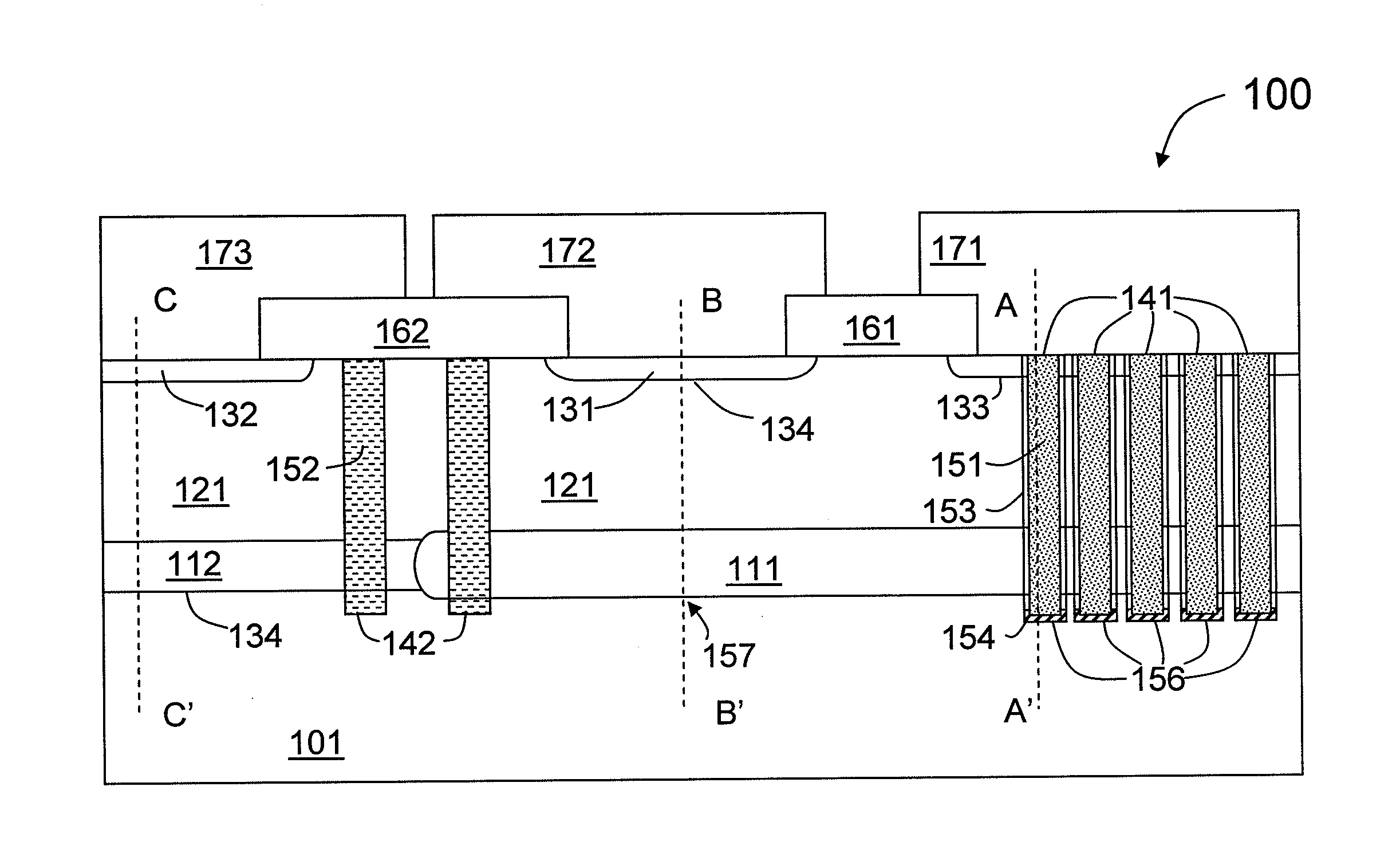
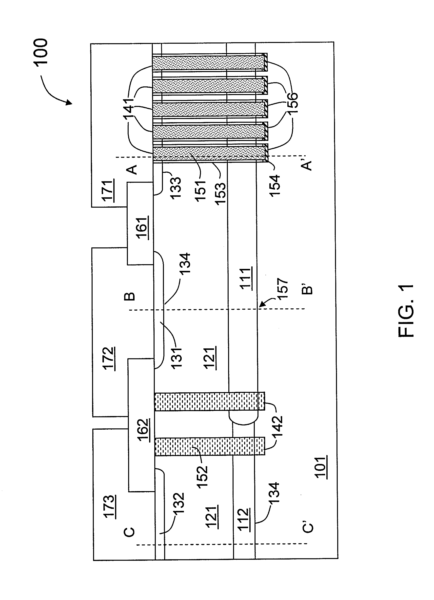
[0031]Embodiments of the present invention are directed to devices and methods for providing transient voltage suppression (TVS) for integrated circuits. Depending on the embodiment, the TVS devices may have one or more of the following features:[0032]1. The TVS structure is able to survive an ESD / Surge event described by IEC 6100-4-2,(ESD) + / −15 kV(air),+ / −8 kV(contact);[0033]2. The TVS structure protects the device under protection from the ESD / Surge event described by IEC 6100-4-2,(ESD) + / −15 kV(air),+ / −8 kV(contact); and[0034]3. The TVS structure does not degrade the signal going to the device under protection.

[0035]The description below will be with reference to a series of drawing figures enumerated above. These diagrams are merely examples, and should not unduly limit the scope of the claims herein. In connection with the various aspects illustrated and described, one of ordinary skill in the art would recognize other variations, modifications, and alternatives.

[0036]FIG. 1 i...


PUM


Abstract

A transient voltage suppressor (TVS) device includes a semiconductor substrate of a first conductivity type, and a first and a second semiconductor regions of a second conductivity type overlying the semiconductor substrate. A semiconductor layer of the second conductivity type overlies the first and the second semiconductor regions. The TVS device has a first trench extending through the semiconductor layer and the first semiconductor region and into the semiconductor substrate, and a fill material of the second conductivity type disposed in the first trench. A clamping diode in the TVS device has a junction between an out-diffused region from the fill material and a portion of the semiconductor substrate. The TVS device also includes a first P-N diode formed in a first portion of the semiconductor layer, and a second P-N diode having a junction between the second semiconductor region and the semiconductor substrate.

Description

CROSS-REFERENCES TO RELATED APPLICATIONS[0001]This application claims priority to Chinese Patent Application No. ______, filed—Apr. 27, 2010, by inventors Francis Hawe et. al., commonly assigned and incorporated in its entirety by reference herein for all purposes.BACKGROUND OF THE INVENTION[0002]Embodiments of the present invention are directed generally to semiconductor devices, and more particularly, devices and methods for providing transient voltage suppression for integrated circuits.[0003]As integrated circuit technology continues to advance, devices are becoming smaller and operating voltages lower. At the same time, the devices are becoming faster and operating frequencies are higher. As a result, it is more difficult for transient voltage suppressor (TVS) or electrostatic discharge (ESD) protection devices to meet these requirements for today's integrated circuits. The TVS or ESD devices must provide a low breakdown voltage and low capacitance to satisfy the low voltage hi...

Claims


Application Information

Patent Timeline
IPC IPC(8): H01L27/08H01L29/861H01L21/329H01L21/70H01L23/60
CPCH01L27/0255H01L29/866H01L29/8611
Inventor HAWE, FRANCIS EDWARDLIANG, JINSUICHENG, XIAOQIANGLIU, XIANFENG
Owner BCD SHANGHAI MICRO ELECTRONICS CO LTD
Why Eureka
Try Eureka