
Symmetrical Electrical Physical Layer Activity Detector

a detector and electrical physical layer technology, applied in the field of analog circuit design, to achieve the effect of excellent common mode rejection

Active Publication Date: 2011-11-03
MICROCHIP TECH INC
View PDF4 Cites 1 Cited by
  • Summary
  • Abstract
  • Description
  • Claims
  • Application Information

AI Technical Summary

Benefits of technology

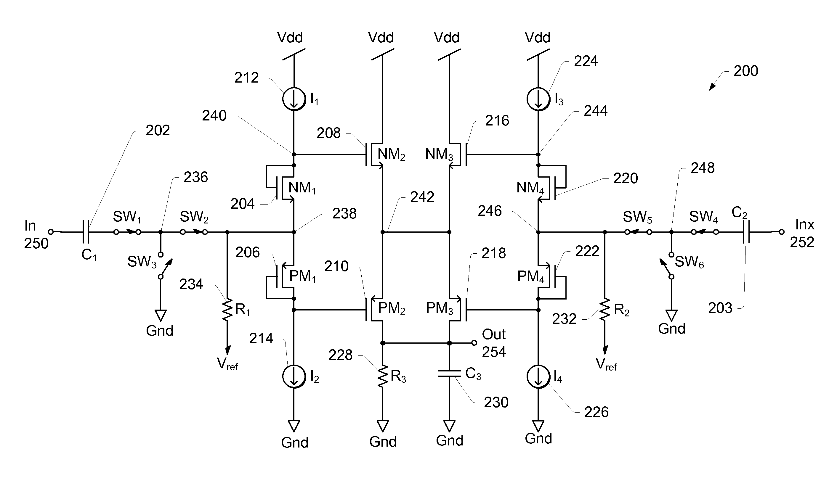
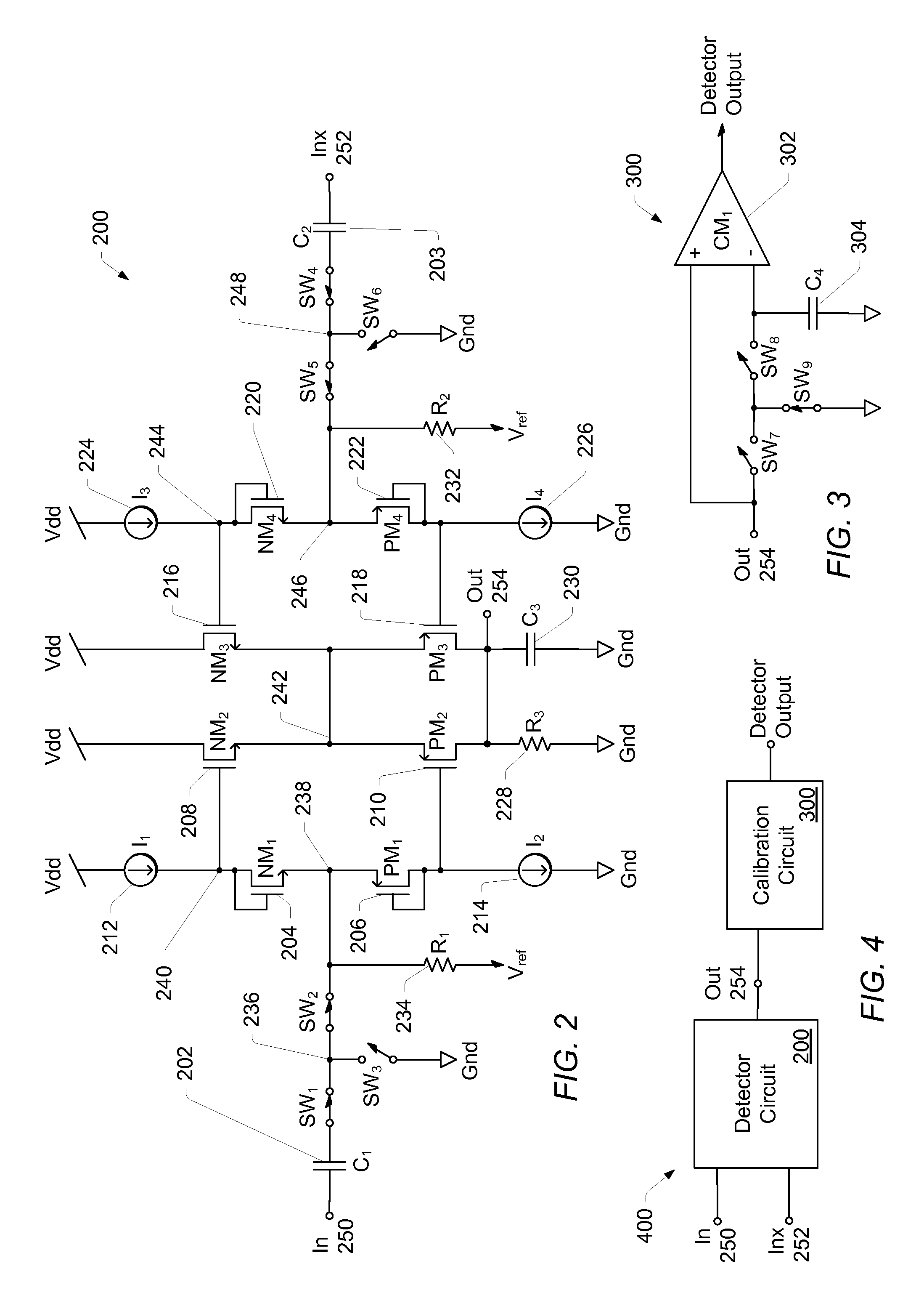
The circuit effectively detects small differential signals while rejecting common mode signals up to 400 MHz and 1V peak-to-peak, with low current consumption, enhancing signal detection efficiency and reducing power usage in MOST networks.

Problems solved by technology

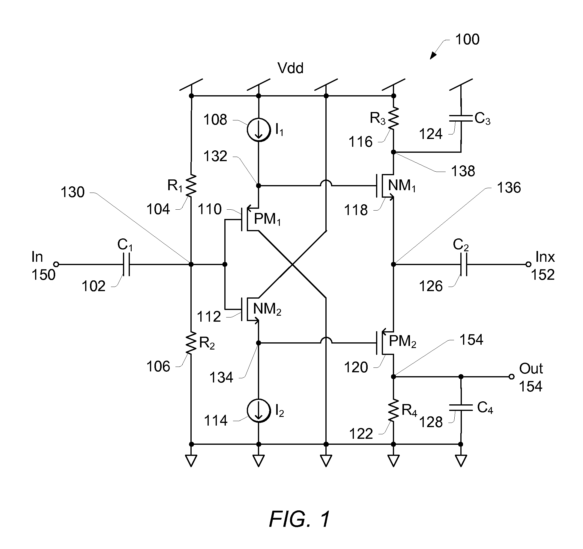
For example, present day detector circuits using a diode, filter, and comparator, typically have problems rejecting common mode signals, and use much more current than the various embodiments of the low-current detector circuit described herein.

Method used


Image

  • Symmetrical Electrical Physical Layer Activity Detector
  • Symmetrical Electrical Physical Layer Activity Detector
  • Symmetrical Electrical Physical Layer Activity Detector

Examples


Embodiment Construction

As used herein, “structure type” refers to the physical structure of an individual resistive element, or resistor implemented on an integrated circuit for a given process. For example, for a given CMOS process a resistor may be implemented to be of one of a variety of structure types, which may include n-diffusion, p-diffusion, n-well, p-well, pinched n-well, pinched p-well, poly-silicon and metal. When configured on an integrated circuit, a single “resistance” may be constructed as a single resistor or as two or more resistors connected together, where each individual resistor may be of a different structure type. When constructed of more than one resistor, the nominal value of the resistance may be equivalent to the sum of the nominal values of the resistors that make up the resistance. A “resistor string” refers to resistances connected in series, with connective taps available at the terminals of the resistances. Similarly, a “capacitance” may be constructed as a single capacito...


PUM


Abstract

A low-current differential signal activity detector circuit may be configured to reject large common mode signals on differential input lines, while still detecting smaller differential signals applied to the same set of differential input lines. The detector circuit may comprise a translinear buffer that is driven at the buffer input and at the buffer output by the differential input signals. The differential signal thereby driving the inputs of the detector circuit may be half-wave rectified through the buffer output devices and may be filtered to provide the detected output. When applying a common mode signal, the buffer's input and output may track each other, and no current may be rectified in the output devices, thus providing common-mode signal rejection. The detector circuit may also be configured with two buffers having their outputs coupled to a common node, each buffer input driven by a respective one of the differential input signals. The differential signal thereby driving the inputs of the detector circuit may be fully rectified through the output devices of the two buffers, and may be filtered to provide the detected output. The two buffers may be configured in a symmetrical structure that allows for the rejection of common-mode signals when the outputs of the buffers are coupled to a common node.

Description

BACKGROUND OF THE INVENTION1. Field of the InventionThis invention relates generally to analog circuit design, and, more particularly, to the design of a detector circuit that consumes low current and can reject large common mode signals while detecting small differential signal activity.2. Description of the Related ArtMedia Oriented Systems Transport (MOST) is a fiber optic network configured for the efficient transport of high volumes of data at low-cost. Due to its typically low-overhead and low-cost interface, MOST is often used for communicating with a wide variety of peripheral devices in the car environment, like microphones and speakers. Overall, MOST is a synchronous network, where a timing master supplies a clock signal with a synchronous and continuous data signal, with all other devices synchronizing their operation to this clock signal. This eliminates the need for buffering, and having to perform sample rate conversion, making it possible to interconnect simple and in...

Claims


Application Information

Patent Timeline
Patent Type & Authority Applications(United States)
IPC IPC(8): H03K5/153
CPCH03F3/45H03F3/3076
Inventor MCLEOD, SCOTT C.
Owner MICROCHIP TECH INC
Learn More