
Magnetic memory element and magnetic random access memory

Active Publication Date: 2011-11-03
NEC CORP
View PDF4 Cites 18 Cited by
  • Summary
  • Abstract
  • Description
  • Claims
  • Application Information

AI Technical Summary

Benefits of technology

[0030]An object of the present invention is to provide a magnetic memory element and a magnetic random access memory having a structure in which magnetization fixed areas and domain wall pinning sites can be easily formed in a current driven domain wall motion MRAM with perpendicular magnetic anisotropy of a magnetization recording layer.
[0034]According to the present invention, a magnetic memory element can be provided, in which magnetization fixed areas and domain wall pinning sites can be easily formed.

Problems solved by technology

When a write current is large, a chip area is necessarily large and power consumed for writing increases.
However, in the current driven domain wall motion MRAM, there is concern that an absolute value of the write current tends to relatively increase.
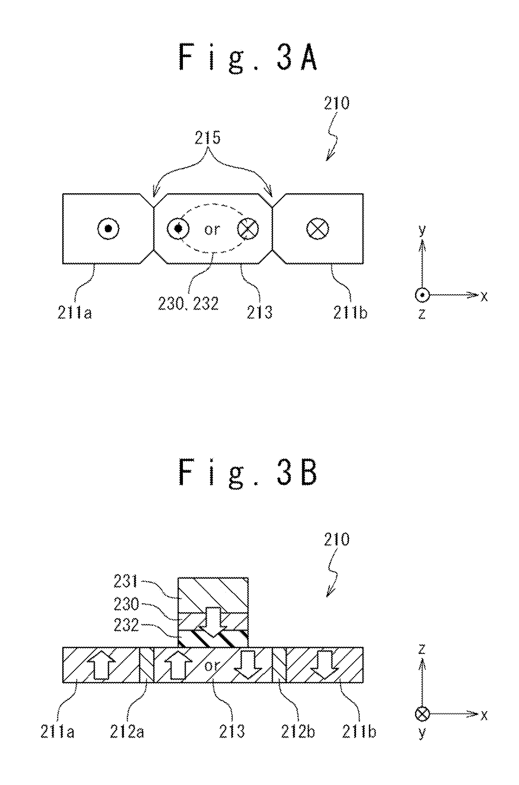
However, as shown in FIGS. 3A and 3B, if the magnetization recording layer has the perpendicular magnetic anisotropy and the magnetization direction is a direction perpendicular to the in-plane direction, even by forming the magnetization recording layer to the U-shape, it is quite difficult to initialize the magnetization directions of the magnetization fixed layers and the position of the domain wall using an external magnetic field.
Therefore, there may be a case that the shape of the constricted portion 215 is deteriorated due to production tolerance.
Therefore, the magneto-resistance effect element cannot function as a magnetic memory cell.
In addition, if the miniaturization of the magneto-resistance effect element advances and the width of the magnetization recording layer thereof may become narrow, it is very difficult to form the constricted portion 215 and there is a possibility to require a fabrication technique beyond the limitation of the lithography technique of the semiconductor processing.

Method used


Image

  • Magnetic memory element and magnetic random access memory
  • Magnetic memory element and magnetic random access memory
  • Magnetic memory element and magnetic random access memory

Examples


Embodiment Construction

[0078]Embodiments of a magnetic memory element and a magnetic random access memory (MRAM) of the present invention will be described below referring to the accompanying drawings.

1. Basic Structure of Magnetic Memory Element

[0079]FIG. 4A is a plan view showing an example of a structure of a magnetization recording layer of a magnetic memory element according to an embodiment of the present invention. FIG. 4B is a sectional view showing an example of a structure of the magnetic memory element according to the embodiment of the present invention. Here, in FIGS. 9A and 4B, a symbol of an open circle and a dot, a symbol of an open circle and a x-mark, and a symbol of an open arrow show magnetization directions of areas where the symbols are drawn as widely used (hereinafter, these are the same in this Specification and Drawings).

[0080]A magnetic Memory element 1 includes: a magnetization recording layer 10; and a magnetic tunneling junction section 20. The magnetization recording layer 1...


PUM


Abstract

A magnetic memory cell includes: a magnetization recording layer; and a magnetic tunneling junction section. The magnetization recording layer includes a ferromagnetic layer with perpendicular magnetic anisotropy. The magnetic tunneling junction section is used for reading information in the magnetization recording layer. The magnetization recording layer includes two domain wall moving areas.

Description

TECHNICAL FIELD[0001]The present invention relates to a magnetic memory element and a magnetic random access memory, and particularly relates to a dome in wall motion magnetic memory element and a domain wall motion magnetic random access memory.BACKGROUND ART[0002]A magnetic random access memory (MRAM) is expected and actively developed as a nonvolatile memory capable of performing a high-speed operation and rewriting an infinite number of times. In the MRAM, a magneto-resistance effect element is integrated in a memory cell and data is stored as a magnetization direction of a ferromagnetic layer in the magneto-resistance effect element. Some types of MRAMs are proposed to meet methods of switching the magnetization direction of the ferromagnetic layer.[0003]A current-induced magnetic field writing MRAM is one of the most general MRAMs. In this MRAM, a wiring line that a write current passes through is installed on the periphery of a magneto-resistance effect element and a magnetiz...

Claims


Application Information

Patent Timeline
IPC IPC(8): G11C11/14
CPCG11C11/16H01L43/08H01L27/228G11C11/1655G11C11/1659G11C11/161G11C11/1673G11C11/1675H10B61/22H10N50/10
Inventor NAGAHARA, KIYOKAZUFUKAMI, SHUNSUKEISHIWATA, NOBUYUKISUZUKI, TETSUHIROOHSHIMA, NORIKAZU
Owner NEC CORP
Learn More