

Photovoltaic Structure And Method Of Fabication Employing Nanowire In Stub
a photovoltaic cell and nanowire technology, applied in the field of photovoltaic devices, can solve the problems of reducing the drift mobility and diffusion of charged carriers, degrading performance, and affecting the production process of final products
- Summary
- Abstract
- Description
- Claims
- Application Information
AI Technical Summary
Benefits of technology
Problems solved by technology
Method used
Image

Examples
Embodiment Construction
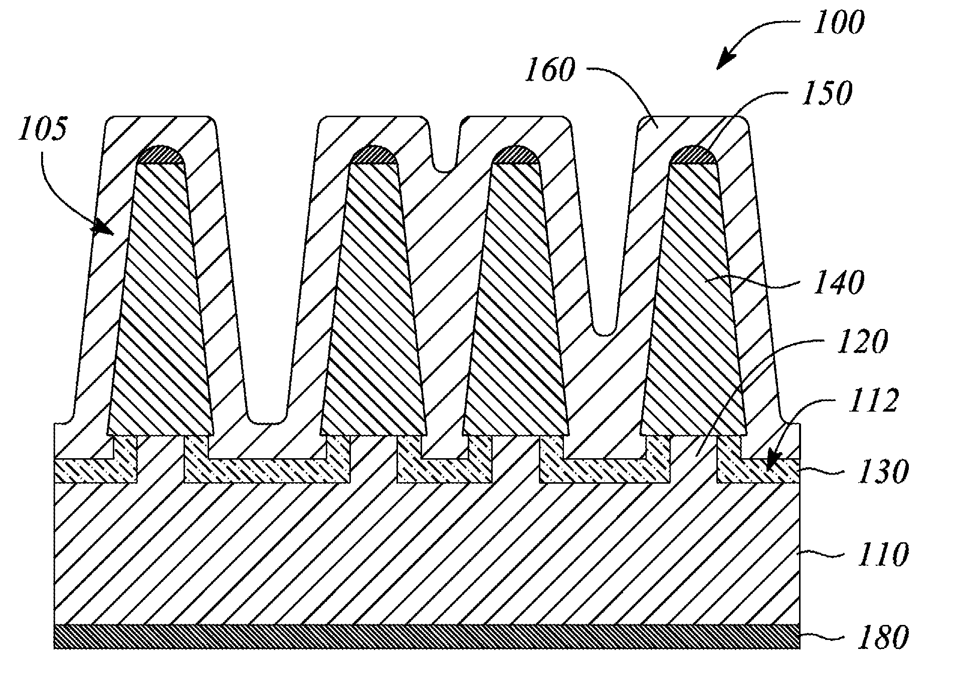
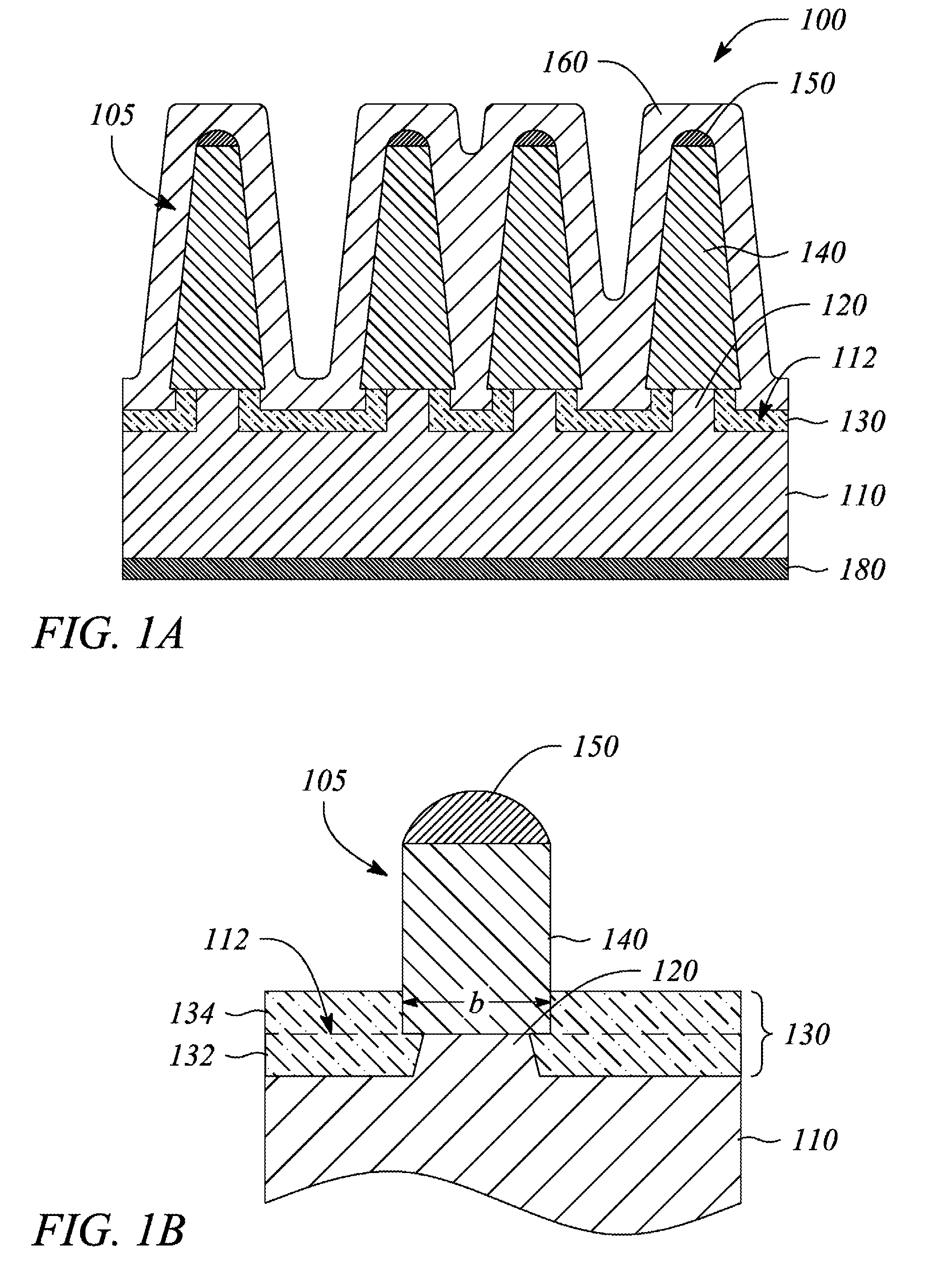
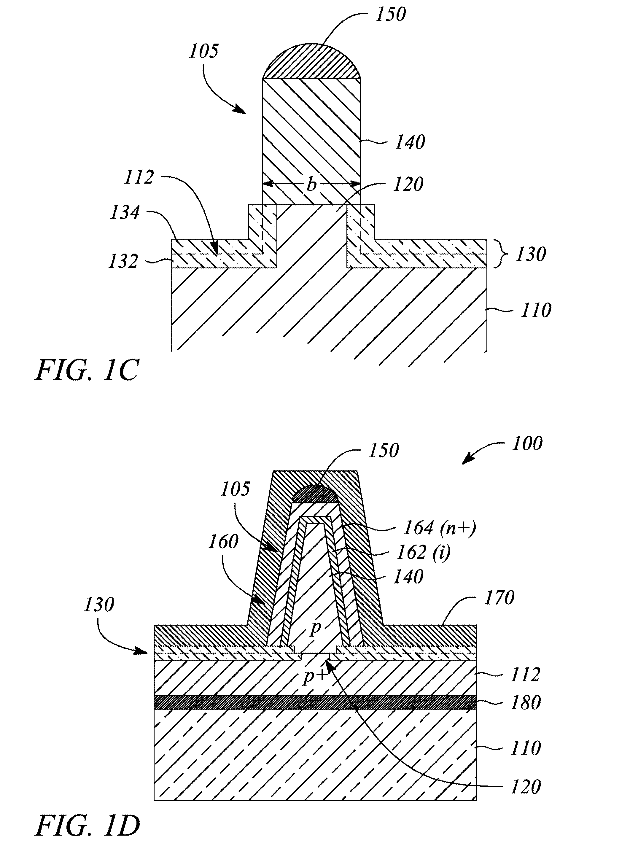
[0020]Embodiments of the present invention provide a photovoltaic structure for a photovoltaic cell that employs a nanowire and a self-aligned nanoscale fabrication approach to make the photovoltaic structure. In particular, the nanowire-based photovoltaic structure provides both built-in electrical isolation and a large contact area to reduce a series resistance of a photovoltaic cell comprising the photovoltaic structure, according to embodiments of the present invention. The nanowire provides greater surface area along its length for a semiconductor junction in the photovoltaic cell. In some embodiments, a plurality of nanowires that has a disordered arrangement in the photovoltaic cell further contributes to increasing the semiconductor junction contact area. Further, the disordered nanowires may facilitate more light absorption by the photovoltaic cell.
[0021]The nanoscale fabrication approach is a self-aligned process that uses no lithography at all or uses no multilayer precis...
PUM
| Property | Measurement | Unit |
|---|---|---|
| temperature | aaaaa | aaaaa |
| temperatures | aaaaa | aaaaa |
| temperature | aaaaa | aaaaa |
Abstract
Description
Claims
Application Information