Switching gate driver

a gate driver and gate technology, applied in the direction of pulse technique, oscillation generator, power conversion system, etc., can solve the problems of decreased switching loss, increased switching loss, increased switching loss, etc., to reduce the voltage rated capacitance of the igbt, shorten the switching time, and reduce the switching loss

Active Publication Date: 2011-11-10
LSIS CO LTD
View PDF2 Cites 47 Cited by
  • Summary
  • Abstract
  • Description
  • Claims
  • Application Information

AI Technical Summary

Benefits of technology

[0026]The present disclosure has an advantage effect in that since the gate driver makes a gate resistor variable according to the collector-emitter voltage Vice of the IGBT device and suppresses a spike voltage of the collector-emitter voltage of the IGBT device occurring when the IGBT device is turned off, it is possible to reduce a switching loss by shortening a switching time compared with that of a gate driver designed with a fixed-gate resistor RG.
[0027]The present disclosure has another advantageous effect in that, it is possible to reduce a voltage rated capacitance of the IGBT by suppressing an IGBT spike voltage of a collector-emitter voltage of the IGBT device, it becomes easy to design a snubber circuit to suppress an IGBT spike voltage by suppressing an IGBT spike voltage of a collector-emitter of the IGBT device, and it becomes easy to design a heat dissipation of an IGBT device by reducing a switching loss when an IGBT device of a collector-emitter voltage Vice of an IGBT device is turned off.

Problems solved by technology

On the other hand, when designing the gate resistors RG(on) and RG(off) in a large magnitude, current change time becomes long so that a switching loss is increased.
However, a switching loss is increased.
When designing the gate resistor RG to be small, gate charge / discharge time for the IGBT device becomes short so that a switching loss is decreased.

Method used


Image

  • Switching gate driver
  • Switching gate driver
  • Switching gate driver

Examples


Embodiment Construction

[0038]Hereinafter, the most preferred embodiment of the present disclosure is given with reference to the accompanying drawings in order to describe the technical idea of the present disclosure to the extent that those skilled in the art can embody the technical idea of the present disclosure with ease.

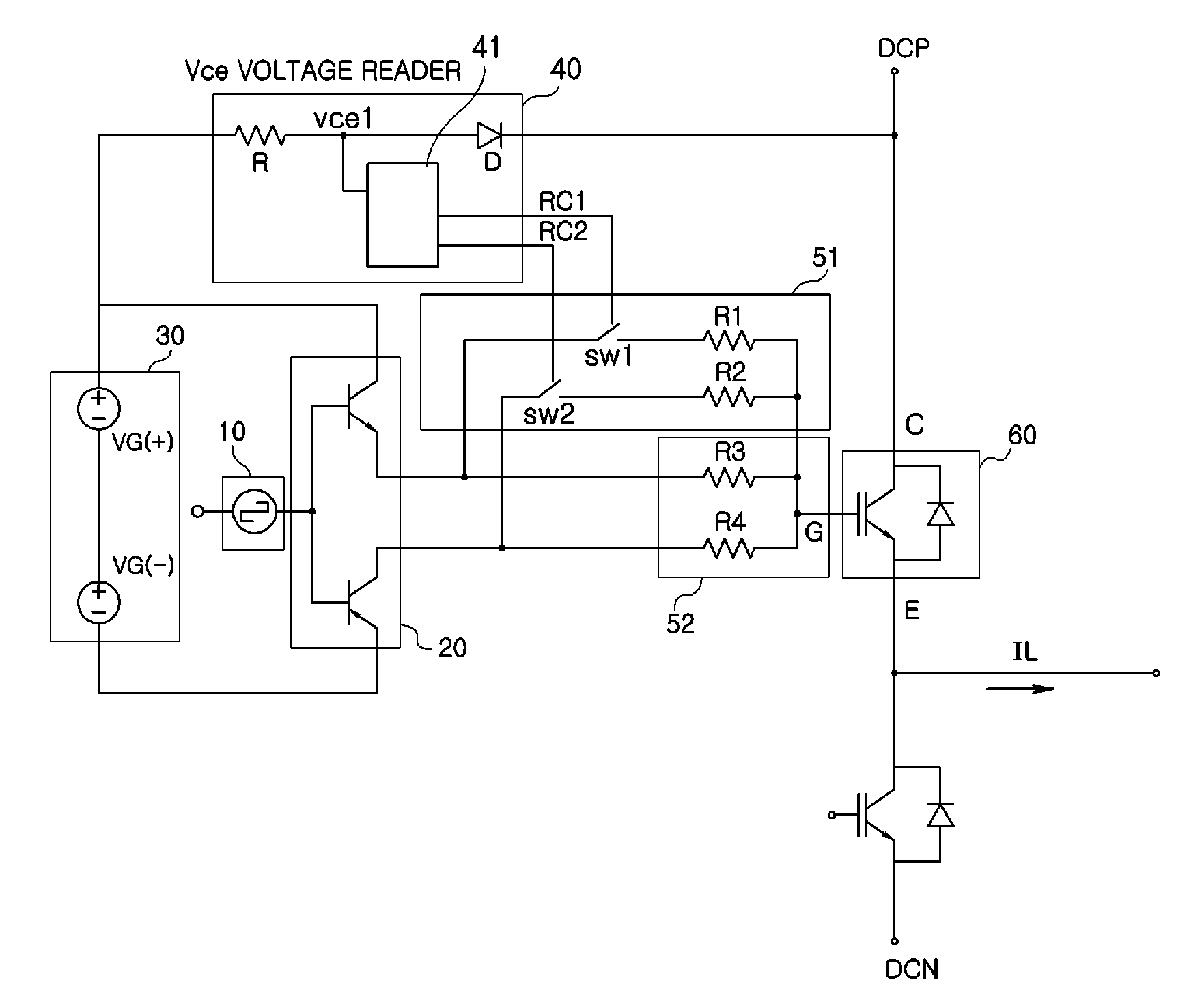
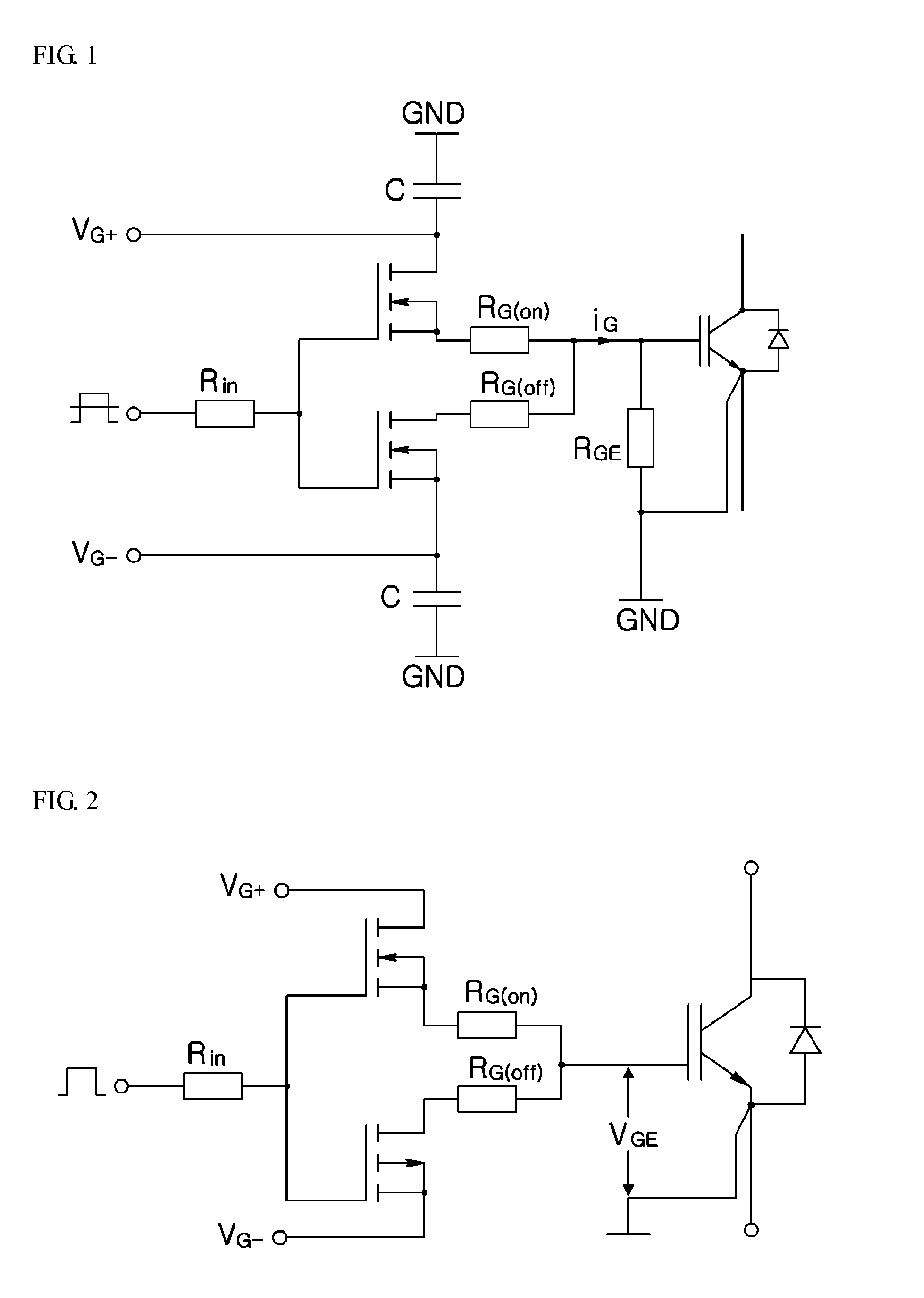
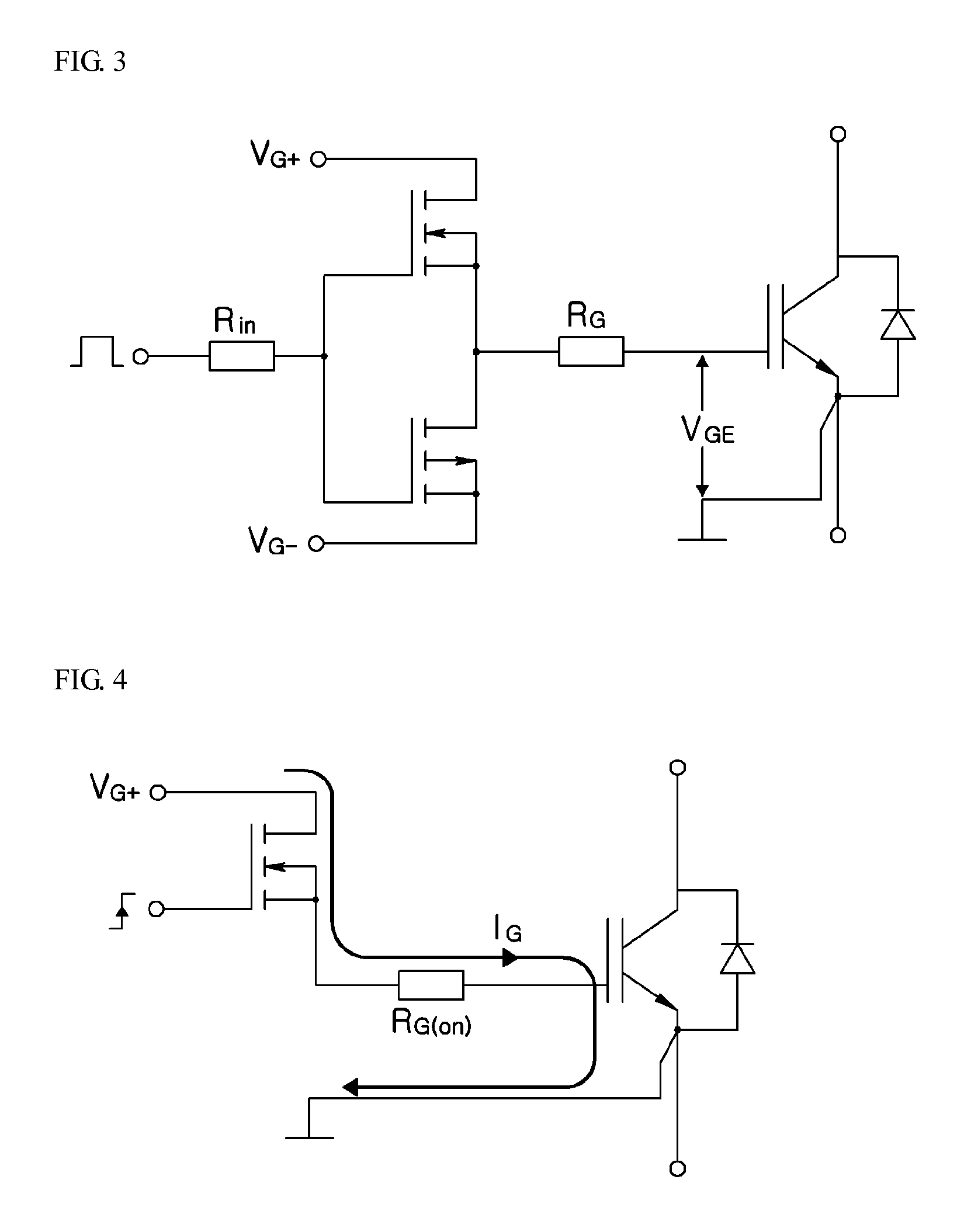
[0039]FIG. 6 is a constructional diagram of an IGBT gate driver in an inverter system. FIG. 7 is a wave form diagram illustrating operational characteristics of IGBT device and MOS FET device. FIG. 8 is a block diagram illustrating a switching gate driver according to an embodiment of the present disclosure. FIG. 9 is a circuit diagram of a switching gate driver illustrated in FIG. 8. FIG. 10 is a circuit diagram illustrating an embodiment of a voltage detection circuit included in a voltage reader. FIG. 11 is a wave form diagram illustrating an operational state of each signal illustrated in FIG. 9. FIGS. 12 and 13 are wave form diagrams illustrating operations of the switching gate ...


PUM


Abstract

Disclosed is a switching gate driver of an IGBT device, including a resistor unit to control a gate current of the IGBT device; and a voltage reader that outputs a control signal to control a variable resistor unit of the resistor unit to the resistor unit, according to a collector-emitter voltage of the IGBT device.

Description

[0001]Pursuant to 35 U.S.C. §119 (a), this application claims the benefit of earlier filing date and right of priority to Korean Patent Application No. 10-2010-0042661, filed on May 6, 2010, the contents of which are hereby incorporated by reference in their entirety.BACKGROUND OF THE DISCLOSURE[0002]1. Field of the Invention[0003]The present disclosure relates to a switching gate driver which is included to drive an inverter, and more particularly, to a switching gate driver to reduce an On / Off switching stress.[0004]2. Description of the Related Art[0005]An inverter is a device that converts an AC voltage to a DC voltage, generates an AC voltage when a switching device switches the converted DC voltage according to a PWM (Pulse Width Modulation) signal, and outputs the generated AC voltage to a load to be driven. It provides the load with an AC voltage having voltage and frequency required by a user so that the driving of the load can be precisely controlled.[0006]An IGBT (Insulat...

Claims


Application Information

Patent Timeline
Patent Type & Authority Applications(United States)
IPC IPC(8): H03K3/00
CPCH02M1/08H03K17/0412H03K2217/0036H03K17/567H03K17/6877H03K17/163
Inventor LEE, JAE MOON
Owner LSIS CO LTD
Why Eureka
Try Eureka