Method of mounting semiconductor chips, semiconductor device obtained using the method,method of connecting semiconductor chips, three-dimensional structure in which wiring is provided on its surface, and method of producing the same

a technology of semiconductor chips and connecting materials, which is applied in the direction of semiconductor/solid-state device testing/measurement, sustainable manufacturing/processing, instruments, etc., can solve the problems of affecting the reliability of the semiconductor device, and often using expensive gold as the wire. , to achieve the effect of inhibiting the breakage or damage of the wir

Active Publication Date: 2011-11-17
PANASONIC CORP
View PDF9 Cites 28 Cited by
  • Summary
  • Abstract
  • Description
  • Claims
  • Application Information

AI Technical Summary

Benefits of technology

[0008]The present invention aims to resolve the foregoing problems in the wiring bonding that was conventionally used for connecting the semiconductor chip disposed on the insulating base material surface to the electrode pad formed on the insulating base material surface, and its object is to form, with an easy process, a wiring capable of inhibiting the breakage or damage of the wire during the sealing performed with the resin seal material.

Problems solved by technology

Thus, the seal material containing large amounts of inorganic filling material as described above has extremely inferior fluidity.
In such case, considerably external force is applied to the wire used for the bonding, and there was a problem in that the reliability of the semiconductor device would be impaired due to the breakage or damage of the wire.
Nevertheless, expensive gold is often used as the wire.
Thus, increasing the wire diameter means increased costs.
In addition, with the wire bonding method, since the wire spacing cannot be narrowed in consideration of the sweep amount of the wire, there is a problem in that the wiring density is low.

Method used


Image

  • Method of mounting semiconductor chips, semiconductor device obtained using the method,method of connecting semiconductor chips, three-dimensional structure in which wiring is provided on its surface, and method of producing the same
  • Method of mounting semiconductor chips, semiconductor device obtained using the method,method of connecting semiconductor chips, three-dimensional structure in which wiring is provided on its surface, and method of producing the same
  • Method of mounting semiconductor chips, semiconductor device obtained using the method,method of connecting semiconductor chips, three-dimensional structure in which wiring is provided on its surface, and method of producing the same

Examples


first embodiment

[0036]The preferred embodiments of the method of mounting a semiconductor chip according to the present invention are now explained with reference to the drawings.

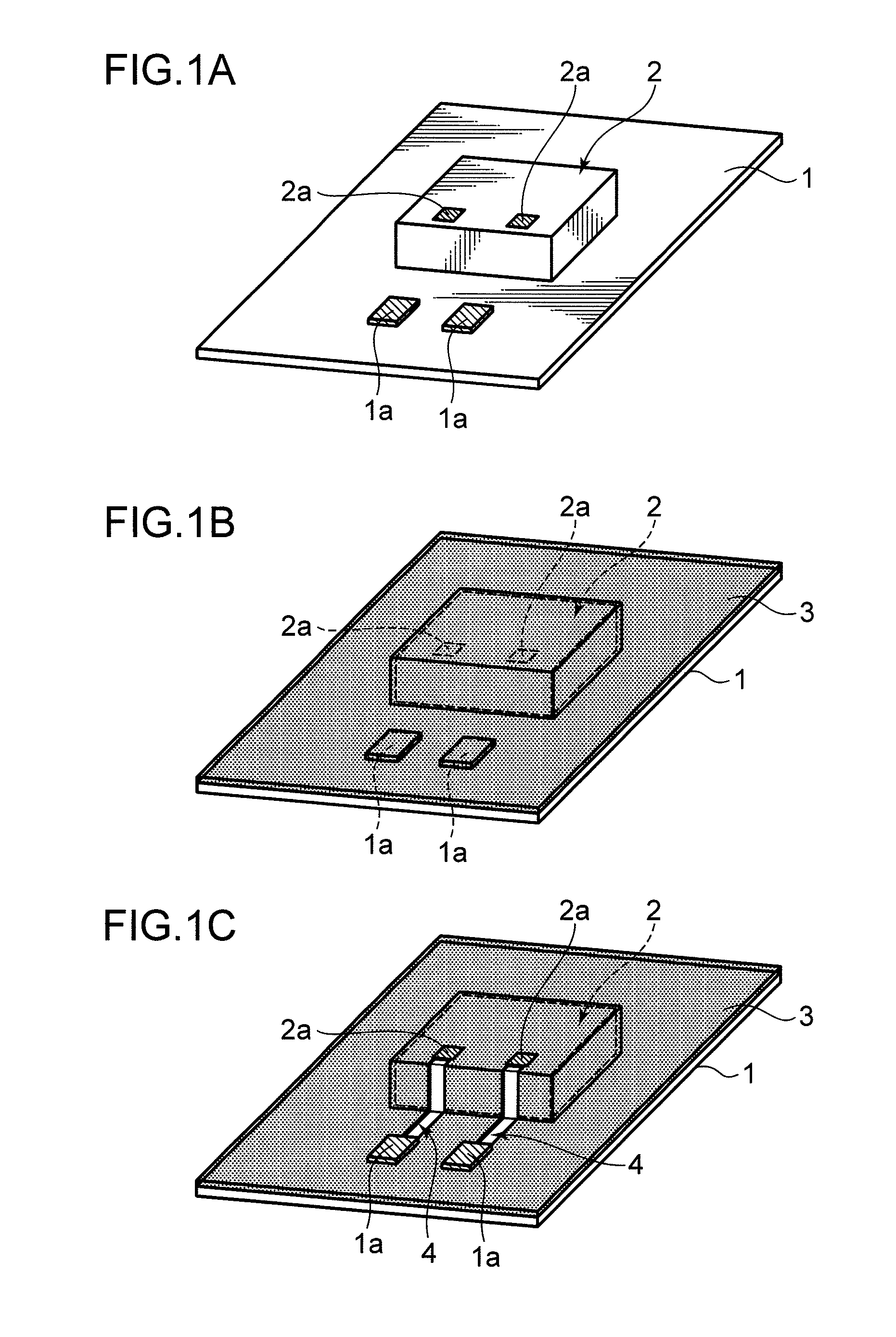
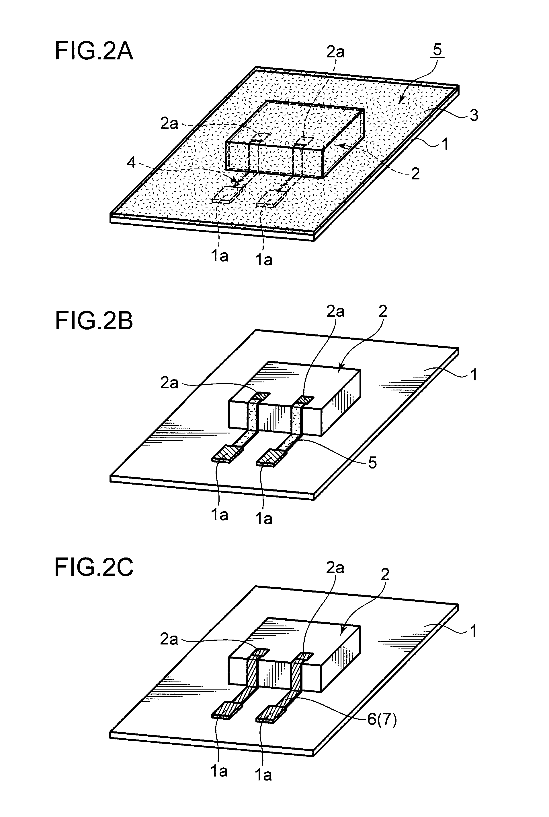
[0037]FIG. 1 and FIG. 2 are schematic diagrams explaining the respective processes in the method of mounting a semiconductor chip of this embodiment. Note that, in FIG. 1 and FIG. 2, 1 represents an insulating base material, 1a represents an electrode pad, 2 represents a semiconductor chip, 2a represents a bonding pad, 3 represents a resin coating, 4 represents a wiring gutter, 5 represents a plating catalyst, 6 represents an electroless plating coating, and 7 represents a wiring.

[0038]In the production method of this embodiment, as shown in FIG. 1A, foremost, an insulating base material 1 mounted with a semiconductor chip 2 in a predetermined chip mounting area is prepared.

[0039]Note that the semiconductor chip 2 is fixed to the predetermined chip mounting area on the surface of the insulating base material 1 using an adh...

second embodiment

[0098]A preferred method of connecting a plurality of semiconductor chips according to the present invention is now explained with reference to the drawings. Note that, since the respective processes are the same as the processes explained in the first embodiment, the detailed explanation of redundant portions is omitted. Moreover, since the components given the same reference numerals as the reference numerals of the first embodiment are the same components, the explanation thereof is omitted.

[0099]FIG. 4 and FIG. 5 are schematic diagrams explaining the respective processes in the method of connecting a plurality of semiconductor chips of this embodiment. In FIG. 4 and FIG. 5, 1 represents an insulating base material, 2 represents a first semiconductor chip, 12 represents a second semiconductor chip, 2a, 12a represent bonding pads, 3 represents a resin coating, 4 represents a wiring gutter, 5 represents a plating catalyst, and 6 represents an electroless plating coating.

[0100]In th...

third embodiment

[0111]According to the method described in the Non-Patent Document 1, a wiring for connecting the insulating base material and the semiconductor chip disposed on a surface of the insulating base material can be formed three-dimensionally across the insulating base material surface and the semiconductor chip surface along the upper surface of the semiconductor chip, the side wall of the semiconductor chip, and the surface of the insulating base material. In other words, the wiring is formed three-dimensionally across two or more adjacent faces on the surface of the three-dimensional structure in which a semiconductor chip is disposed on the surface of the insulating base material. Accordingly, the three-dimensional wiring formed as described above will be stronger than the wiring formed based on wire bonding since it is formed in a manner of creeping along the surface while being in contact with the surface of the insulating base material and the semiconductor chip, and is able to in...


PUM

PropertyMeasurementUnit
thicknessaaaaaaaaaa
diameteraaaaaaaaaa
thicknessaaaaaaaaaa

Abstract

One aspect of the present invention is a method of mounting a semiconductor chip having: a step of forming a resin coating on a surface of a path connecting a bonding pad on a surface of a semiconductor chip and an electrode pad formed on a surface of an insulating base material; a step of forming, by laser beam machining, a wiring gutter having a depth that is equal to or greater than a thickness of the resin coating along the path for connecting the bonding pad and the electrode pad; a step of depositing a plating catalyst on a surface of the wiring gutter; a step of removing the resin coating; and a step of forming an electroless plating coating only at a site where the plating catalyst remains. Another aspect of the present invention is a three-dimensional structure in which a wiring is formed on a surface, wherein, on the surface of the three-dimensional structure, a recessed gutter for wiring is formed, extending between mutually intersecting adjacent faces of the three-dimensional structure, and wherein at least a part of a wiring conductor is embedded in the recessed gutter for wiring.

Description

TECHNICAL FIELD[0001]The present invention relates to a method of mounting a semiconductor chip on an insulating base material surface, a semiconductor device obtained by using the foregoing method, a method of connecting a plurality of semiconductor chips disposed on an insulating base material surface, a three-dimensional structure such as a semiconductor device in which a wiring is provided on its surface, and a method of producing such as a three-dimensional structure.BACKGROUND ART[0002]Conventionally, a semiconductor device in which a semiconductor chip is mounted on an insulating base material is well known. As the method of mounting a semiconductor chip on an insulating base material and electrically connecting the semiconductor chip to an electrode pad formed on the insulating base material surface, the wire bonding method is widely used.[0003]The wire connection method based on wire bonding is a method, as shown in FIG. 6, of mutually connecting a bonding pad 22a formed on...

Claims


Application Information

Patent Timeline
Patent Type & Authority Applications(United States)
IPC IPC(8): G11B5/33H01L21/58H01L23/48H01L21/66
CPCH01L22/12H01L23/3121H01L24/24H01L24/25H01L24/82H01L25/0655H01L25/0657H01L25/50H01L2224/16227H01L2224/16237H01L2224/24051H01L2224/24137H01L2224/24226H01L2224/25175H01L2224/48091H01L2224/48227H01L2224/85H01L2225/06524H01L2225/06551H01L2225/06565H01L2924/01004H01L2924/01005H01L2924/01011H01L2924/01012H01L2924/01013H01L2924/01015H01L2924/0102H01L2924/01027H01L2924/01029H01L2924/0103H01L2924/01033H01L2924/01046H01L2924/01051H01L2924/01056H01L2924/01057H01L2924/01058H01L2924/01075H01L2924/01078H01L2924/01079H01L2924/01082H01L2924/09701H01L2924/12044H01L2924/14H01L2924/19041H01L2924/19043H01L24/48H01L2924/01006H01L2924/01019H01L2924/01023H01L2924/01042H01L2924/01047H01L2924/014H01L2224/24146H01L24/83H01L2224/24011H01L2224/2405H01L2224/245H01L2224/32225H01L2224/82039H01L2224/82101H01L2224/82931H01L2224/82947H01L2224/8385H01L2224/92244H01L2224/82009G11B5/486H05K1/111H05K1/181H05K2201/0376H05K2201/09472H05K3/184H01L2924/00015H01L2924/01014H01L2924/01028H01L24/03H01L24/05H01L21/565H01L2924/10253H01L2924/12041H01L2224/16225H05K1/117H05K1/11H01L24/32H01L2224/73267H01L2224/04042H01L2924/1461Y10T428/1171H01L2924/00014H01L2924/00012H01L2224/45147H01L2224/45144H01L2924/00H01L2924/15787H01L2924/12042H01L2224/05554H01L24/45H01L2924/181H01L24/49H01L2224/49175Y02P70/50H01L2224/82951H01L2224/45015H01L2924/207H01L23/52H01L23/48
Inventor YOSHIOKA, SHINGOFUJIWARA, HIROAKI
Owner PANASONIC CORP
Why Eureka
Try Eureka