Method for manufacturing module with planar coil, and module with planar coil

a manufacturing module and planar coil technology, applied in the direction of magnets, waveguide devices, magnetic bodies, etc., can solve the problems of increasing the manufacturing cost of printed wiring boards with built-in inductor, and the inability to cope with a large current, so as to reduce the manufacturing cost

Active Publication Date: 2011-11-24
MURATA MFG CO LTD
View PDF2 Cites 39 Cited by
  • Summary
  • Abstract
  • Description
  • Claims
  • Application Information

AI Technical Summary

Benefits of technology

[0018]According to a preferred embodiment of the present invention, it is possible to provide a method for manufacturing a module including a planar coil, and a module including a planar coil, capable of reducing manufacturing cost and also coping with a large current.

Problems solved by technology

However, in the case of the conventional printed wiring board with a built-in inductor shown in FIG. 10, a significant amount of time and work is required to form the counterbore section 1b in the printed wiring board 1 for the purpose of mounting the coil 2, thereby increasing manufacturing cost of the printed wiring board 1 with a built-in inductor.
Moreover, since the coil 2 is formed of a winding, it cannot cope with a large current.

Method used


Image

  • Method for manufacturing module with planar coil, and module with planar coil
  • Method for manufacturing module with planar coil, and module with planar coil
  • Method for manufacturing module with planar coil, and module with planar coil

Examples


first preferred embodiment

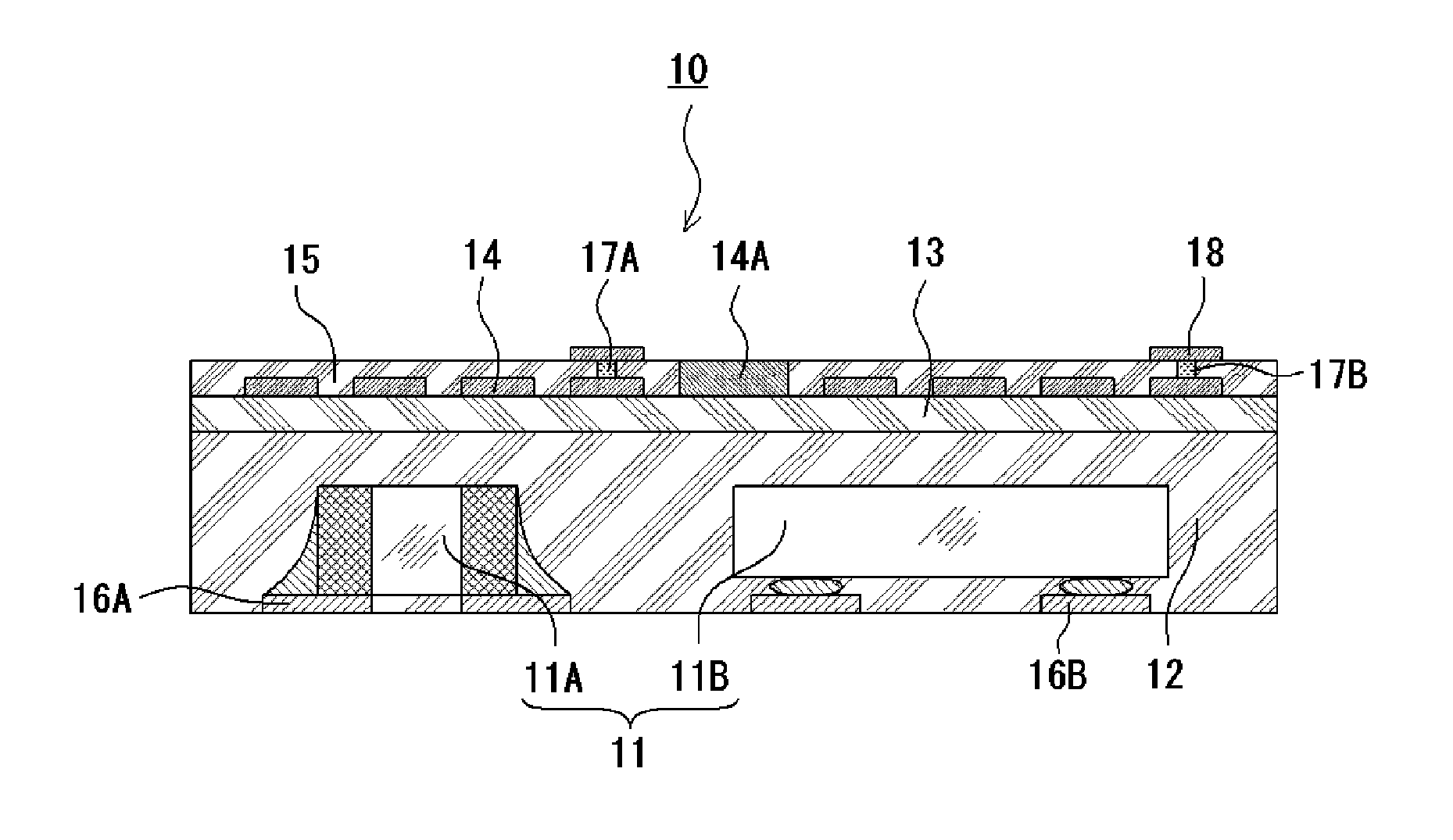
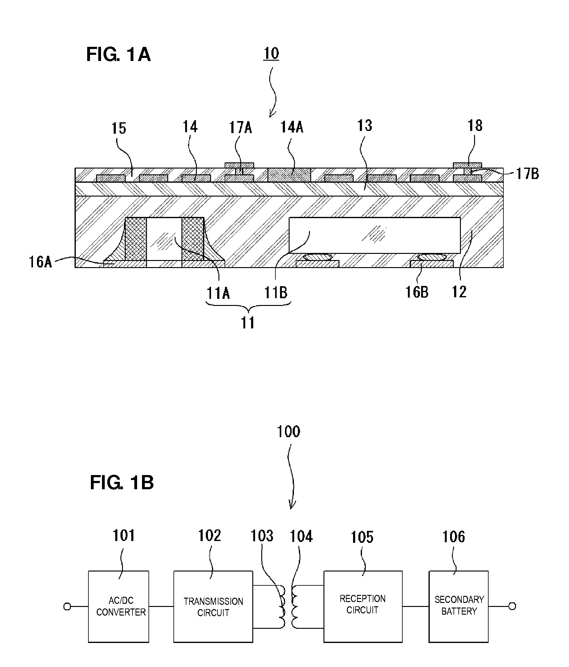
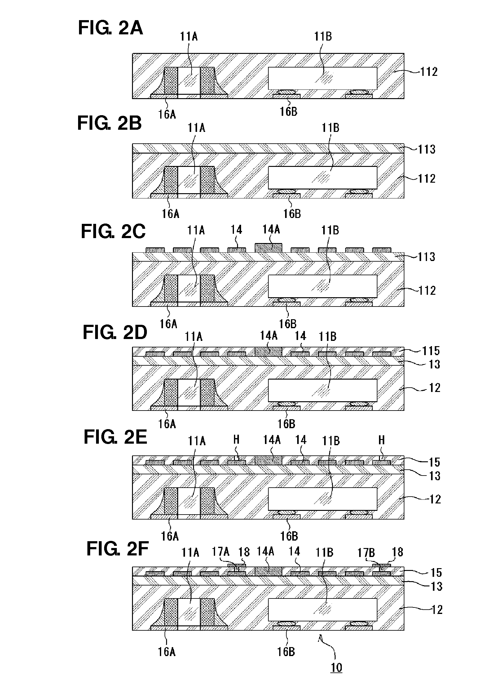
[0032]A module 10 including a planar coil of the present preferred embodiment preferably includes a first resin layer 12 including a built-in chip-type electronic component 11; a second resin layer 13 arranged on the first resin layer 12 and containing a magnetic filler; a spiral planar coil 14 arranged on the second resin layer 13; and a third resin layer 15 including a non-magnetic property and coating the planar coil 14, for example as shown in FIG. 1A, the module 10 preferably being configured as a non-contact type electric power transmission module 100, for example as shown in FIG. 1B.

[0033]Further, as shown in FIG. 1A, a magnetic core 14A is arranged in a central portion (core portion) of the spiral of the planar coil 14, and the magnetic core 14A preferably has a larger thickness than a thickness of the planar coil 14. The planar coil 14 is buried inside the third resin layer 15, while the top surface of the magnetic core 14A is exposed from the top surface of the third resin...

second preferred embodiment

[0056]A module 10A including a planar coil in the present preferred embodiment is configured in a similar manner to the module 10 including the planar coil in the first preferred embodiment except that the configurations of the via hole conductors 17A, 17B are different, for example as shown in FIG. 3. Therefore in the present preferred embodiment, identical or corresponding portions to those in the first preferred embodiment are described as provided with identical numerals.

[0057]In the present preferred embodiment, the via hole conductors 17A, 17B penetrate the first and second resin layers 12, 13, and are connected to the under surfaces of the inner end and the outer end of the planar coil 14. Therefore, routing wiring that connects the via hole conductors 17A, 17B is formed on the side of the substrate (not shown), such as the mother board, which is mounted with the module 10A including the planar coil. This routing wiring may be provided on the under surface of the first resin ...

third preferred embodiment

[0060]A module 10B including a planar coil in the present preferred embodiment is configured basically in a similar manner to the module 10A including the planar coil (see FIG. 3) in the second preferred embodiment except that a shield layer 19 is provided on an interface between the first and second resin layers 12, 13, and a second via hole conductor 17C is electrically connected to this shield layer 19 as a grounding conductor, for example, as shown in FIG. 4. It is to be noted that also in the present preferred embodiment, identical or corresponding portions to those in the second preferred embodiment are described as provided with identical numerals.

[0061]In the case of providing a plated film or metal foil as the shield layer 19, after provision of the plated film or the metal foil throughout the top surface of the second resin layer 13, patterning is performed preferably by a photolithography technique, for example, so that holes to be penetrated by the via hole conductors 17...


PUM

PropertyMeasurementUnit
magnetic propertyaaaaaaaaaa
non-magnetic propertyaaaaaaaaaa
magneticaaaaaaaaaa

Abstract

A method for manufacturing a module including a planar coil, and a module including a planar coil, reduce manufacturing cost and also are able to handle a large current. The method for manufacturing the module including the planar coil includes the steps of providing a second resin layer including a magnetic filler on a first resin layer with a built-in chip-type electronic component; providing a planar coil on the second resin layer; and providing a third resin layer including a non-magnetic property so as to coat the planar coil.

Description

BACKGROUND OF THE INVENTION[0001]1. Field of the Invention[0002]The present invention relates to a method for manufacturing a module including a planar coil, and a module including a planar coil.[0003]2. Description of the Related Art[0004]For example in Japanese Patent Application Laid-Open No. H7-283029, a printed wiring board with a built-in inductor is proposed. This printed wiring board with a built-in inductor will be described based on FIG. 10. As shown in FIG. 10, a through hole 1a in a predetermined shape is formed in a printed wiring board 1. An annular counterbore section 1b is formed outside the through hole 1a, and an annular insulating wall 1c lies between the counterbore section 1b and the through hole 1a. A coil 2 is mounted on the counterbore section 1b. A winding coated with an insulating film is wound to form the coil 2. Further, a first core member 3a with a plain plate is mounted with respect to the through hole 1a in the printed wiring board 1 from the lower su...

Claims


Application Information

Patent Timeline
Patent Type & Authority Applications(United States)
IPC IPC(8): H01F38/14H03H7/01B05D5/12H01F27/02
CPCH01F27/327H01P11/003H01F38/14H01F27/2871Y10T29/4902H01L2224/16227H01L2224/96H01L2224/04105H01L2924/19105
Inventor HATASE, MINORU
Owner MURATA MFG CO LTD
Why Eureka
Try Eureka