
Anodic wafer bonding method, method of manufacturing packages, method of manufacturing piezoelectric vibrators, oscillator, electronic apparatus, and radio clock

a piezoelectric vibrator and anodic wafer technology, applied in the direction of generators/motors, layered products, chemistry apparatuses and processes, etc., can solve the problems of inability to achieve anodic wafer bonding of the pair of wafers, damage to bonding film, etc., to improve the yield ratio of high-quality piezoelectric vibrators, improve quality, and improve the effect of quality

Inactive Publication Date: 2011-11-24
SEIKO INSTR INC
View PDF3 Cites 2 Cited by
  • Summary
  • Abstract
  • Description
  • Claims
  • Application Information

AI Technical Summary

Benefits of technology

In the anodic wafer bonding method according to the present invention, a current value flowing per point can be reduced by applying the voltage to the bonding film from a plurality of points. Therefore, the bonding film 35 can be prevented from being damaged by a heavy current, so that the anodic wafer bonding between the first substrate and the second substrate is ensured. Also, by setting the number of points where the voltage is applied according to the size of the substrates to be anodically bonded, the anodic wafer bonding with high reliability is achieved irrespective of the size of the substrates. In addition, since the bonding film can be prevented from being damaged, a yield ratio can be improved.
In the anodic wafer bonding method according to the present invention, the current value flowing per point can be reduced by applying the voltage to the bonding film from a plurality of points. Therefore, the bonding film can be prevented from being damaged by a heavy current, so that the anodic wafer bonding between the first substrate and the second substrate is ensured. Also, by setting the number of points where the voltage is applied according to the size of the substrates to be anodically bonded, anodic wafer bonding with high reliability is achieved irrespective of the size of the substrates. In addition, since the bonding film can be prevented from being damaged, the yield ratio can be improved.

Problems solved by technology

However, when the heavy current is passed to one point, the bonding film may be damaged due to occurrence of temperature rise, discoloration, burning or the like.
Therefore, there is a problem that if the diameter of the wafer is enlarged, the anodic wafer bonding of the pair of wafers is not achieved.

Method used


Image

  • Anodic wafer bonding method, method of manufacturing packages, method of manufacturing piezoelectric vibrators, oscillator, electronic apparatus, and radio clock
  • Anodic wafer bonding method, method of manufacturing packages, method of manufacturing piezoelectric vibrators, oscillator, electronic apparatus, and radio clock
  • Anodic wafer bonding method, method of manufacturing packages, method of manufacturing piezoelectric vibrators, oscillator, electronic apparatus, and radio clock

Examples


Embodiment Construction

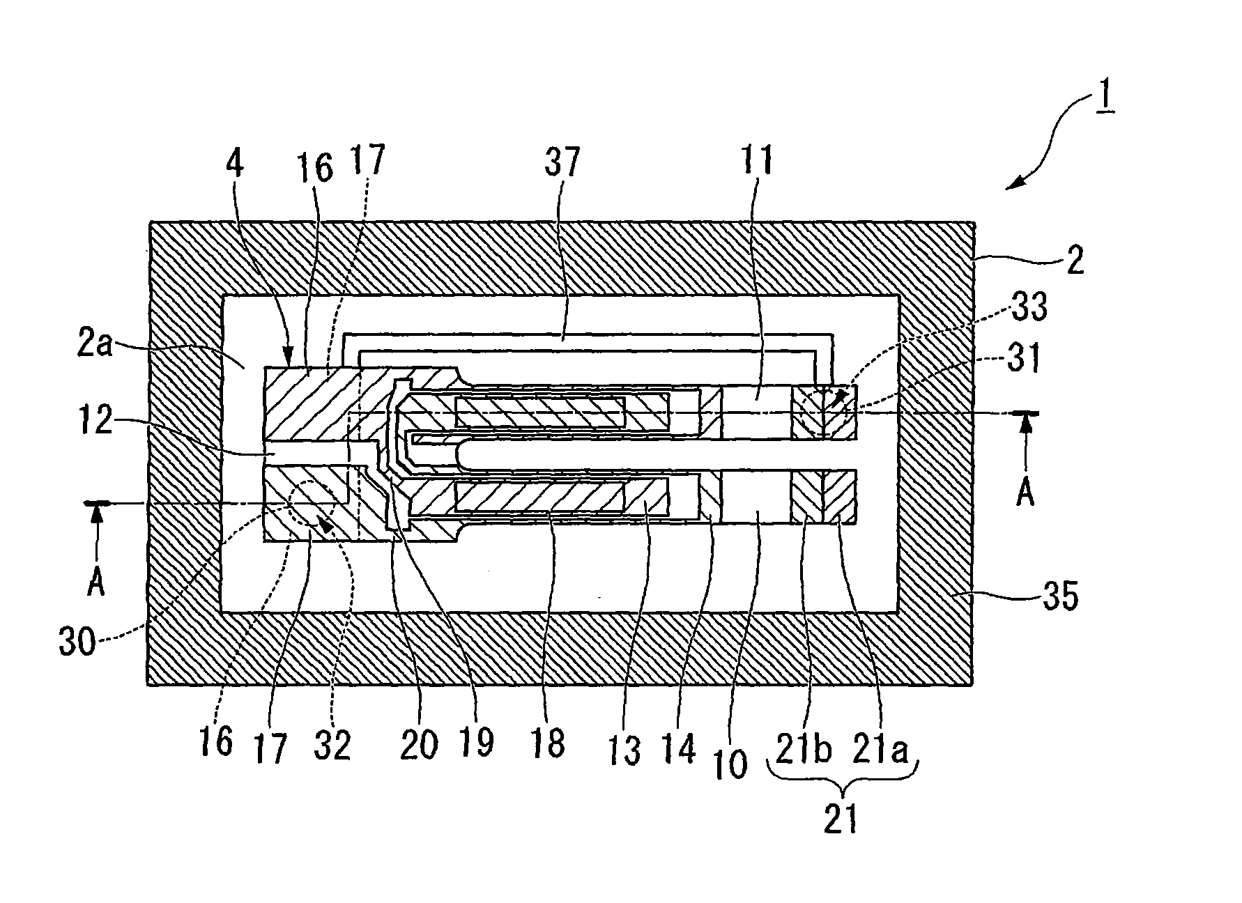
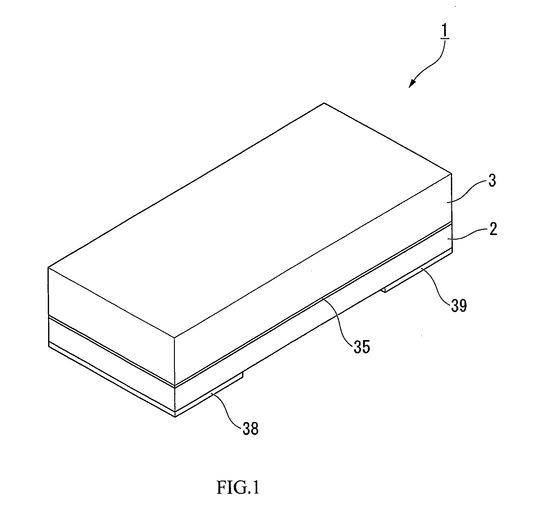
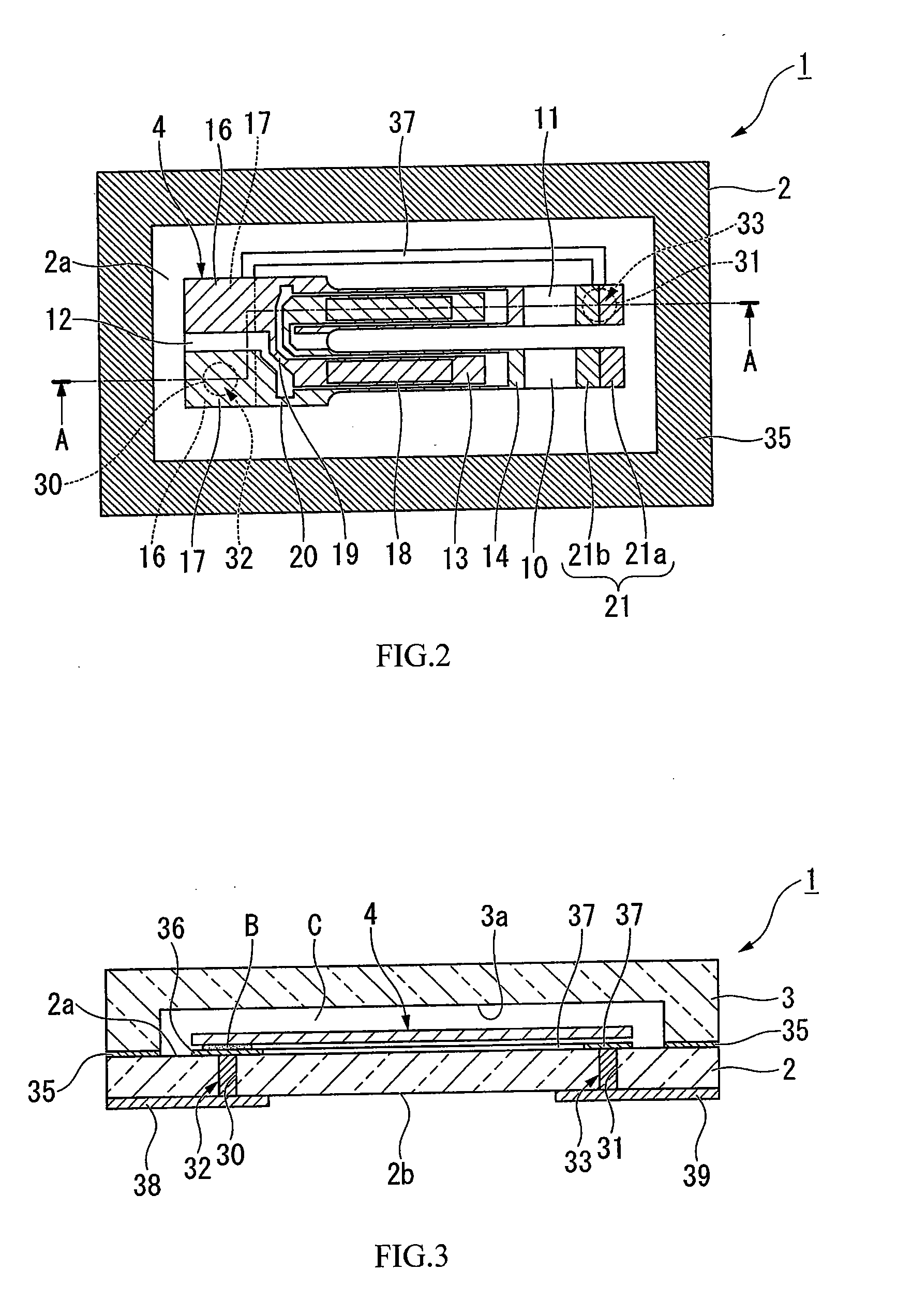
Referring now to FIG. 1 to FIG. 17, an embodiment according to the present invention will be described. In this embodiment, a piezoelectric vibrator in which a base substrate and a lid substrate are laminated, and a piezoelectric vibration reed is mounted in a cavity formed between the substrates, and a method of manufacturing the same will be described.

As shown in FIG. 1 to FIG. 4, a piezoelectric vibrator 1 in this embodiment is a piezoelectric vibrator of a surface mount type, which is formed into a box shape with a base substrate 2 and a lid substrate 3 laminated into two layers, and including a piezoelectric vibration reed 4 stored in a cavity C in the interior thereof. In FIG. 4, for the sake of easy understanding of the drawing, illustration of an excitation electrode 15 of the piezoelectric vibration reed 4, drawn electrodes 19, 20, mount electrodes 16, 17, and a weight metal film 21, described later, is omitted.

As shown in FIG. 5 to FIG. 7, the piezoelectric vibration reed ...


PUM

PropertyMeasurementUnit
Electric potential / voltageaaaaaaaaaa

Abstract

An anodic wafer bonding method according to the present invention is an anodic wafer bonding method for bonding a first substrate formed of an insulating material or a dielectric material and a second substrate which can be anodically bonded by applying a voltage to a bonding film formed of a conductive material formed between the substrates in a state in which the first substrate and the second substrate are laminated, in which the voltage is applied to the bonding film from a plurality of points at the time of anodic wafer bonding.

Description

BACKGROUND OF THE INVENTION1. Field of the InventionThe present invention relates to an anodic wafer bonding method for anodically bonding by applying a voltage to a bonding film formed between a pair of members, a method of manufacturing packages using anodic wafer bonding, a method of manufacturing piezoelectric vibrators, an oscillator, an electronic apparatus, and a radio clock.2. Description of the Related ArtIn recent years, a piezoelectric vibrator using crystal or the like as a time instance source, a timing source of control signals or the like, a reference signal source, and so on in mobile phone sets or portable digital assistant terminal is used. Various types of such piezoelectric vibrators are known, and a piezoelectric vibrator of surface mount device type is known as one of these piezoelectric vibrators. As the piezoelectric vibrator of this type, a three-layer structure type in which a base substrate and a lid substrate are bonded to piezoelectric substrate formed w...

Claims


Application Information

Patent Timeline
IPC IPC(8): H01L41/00B32B38/10B32B37/06
CPCC03C27/06H01L21/50H01L23/10H01L2924/01079H01L2924/3011Y10T156/1052H03H9/21H01L2924/0002H01L2924/16152H03H9/1021H01L2924/00
Inventor ARATAKE, KIYOSHI
Owner SEIKO INSTR INC
Learn More