Patterning method

a patterning and pattern technology, applied in the field of semiconductor process, can solve the problems of double patterning process, difficult scaling down line width or peach of a pattern beyond 22 nm, and high cost of replacing existing equipment with new machines for this purpose, so as to reduce cycle time and process cost. the effect of greatly reducing the line width

Inactive Publication Date: 2011-12-01
UNITED MICROELECTRONICS CORP
View PDF4 Cites 355 Cited by
  • Summary
  • Abstract
  • Description
  • Claims
  • Application Information

AI Technical Summary

Benefits of technology

As mentioned above, the patterning method in the present invention is implemented by directly forming the spacers on the sidewalls of the patterned photoresist layer. Since the spacers are utilized as the mask for transferring the patterns to the mask layer after the removal of the patterned ph

Problems solved by technology

In the current state of lithography process, it is known that scaling down line width or peach of a pattern beyond 22 nm is rather difficult, unless a light source having an extremely shorter wavelength and a corresponding photoresist are used.
Although utilizing a light source with a shorter wavelength is one way to improve the resolution, it is v

Method used


Image

  • Patterning method
  • Patterning method
  • Patterning method

Examples


Embodiment Construction

Reference will now be made in detail to the present preferred embodiments of the invention, examples of which are illustrated in the accompanying drawings. Wherever possible, the same reference numbers are used in the drawings and the description to refer to the same or like parts.

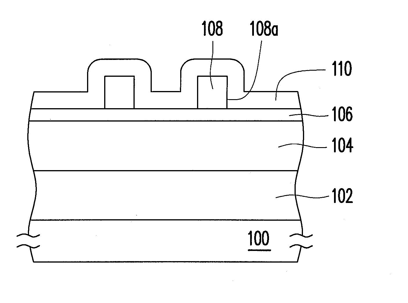
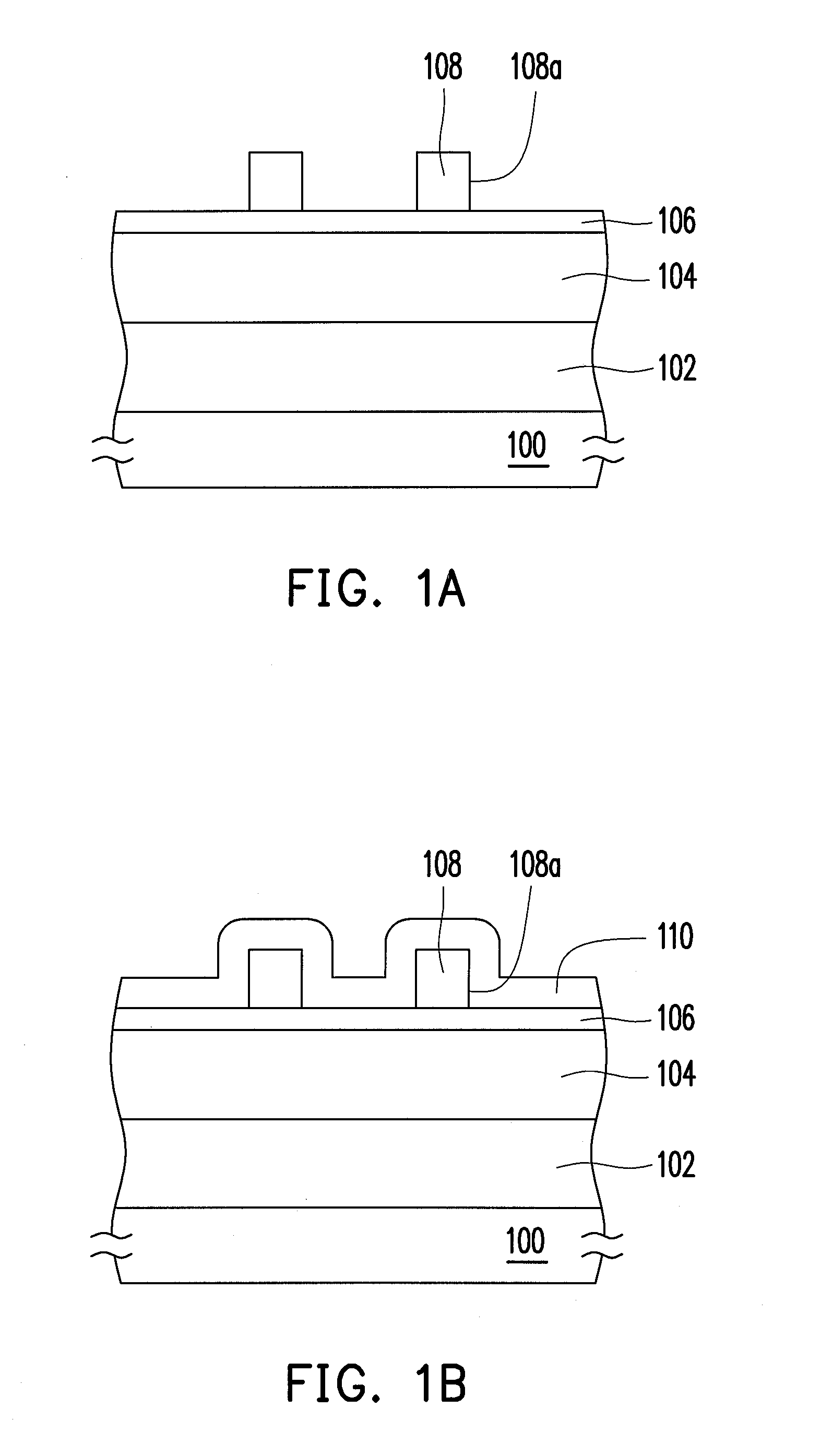
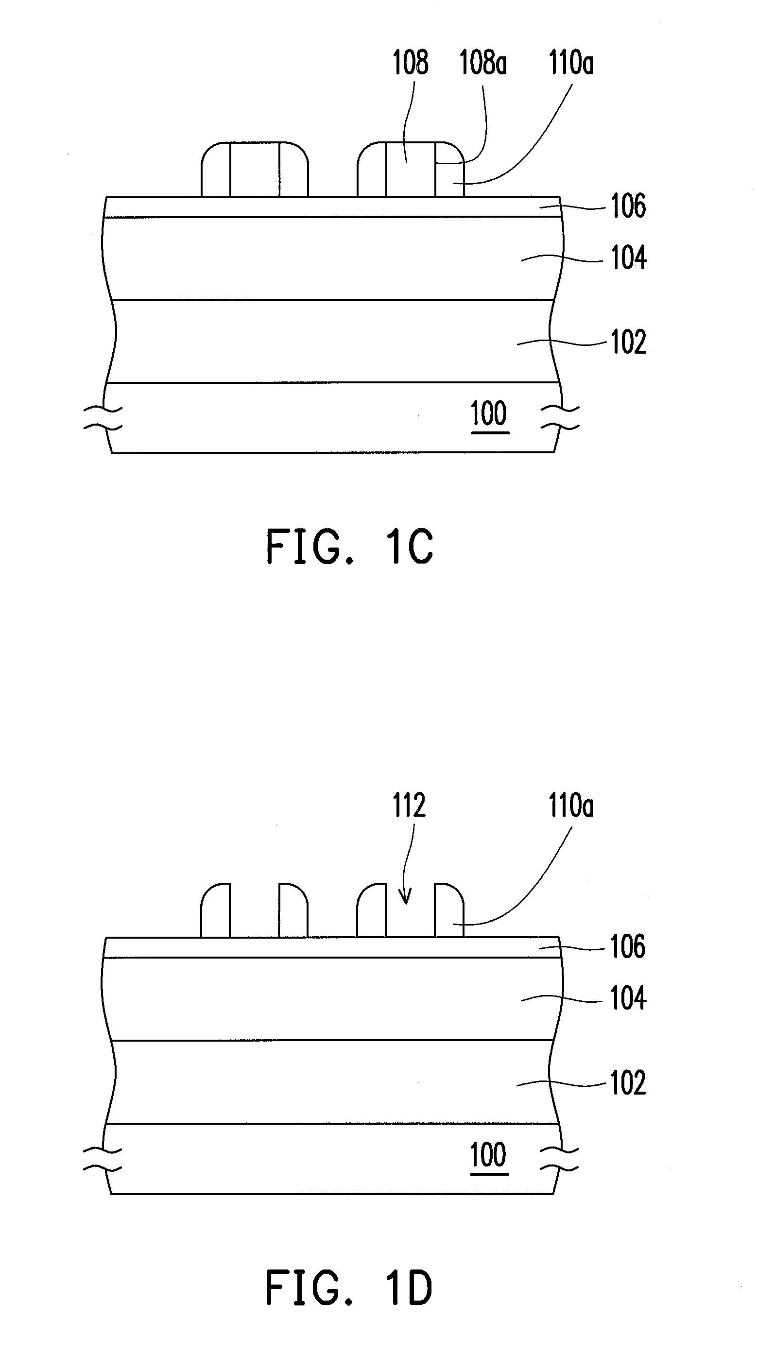
FIGS. 1A-1F depict, in a cross-sectional view, a patterning method according to an embodiment of the present invention. For illustration purposes, the following disclosure is described in terms of line patterns, which are illustrated only as an exemplary example, and should not be adopted for limiting the scope of the present invention. The arrangement or the layout of the patterns to be formed is not particularly limited by the present invention, whereas people skilled in the art should be able to embody the invention based on the illustration to obtain desirable devices with well-patterned structures.

Referring to FIG. 1A, a target layer 102 is provided, which can be formed on a substrate 100. The substra...


PUM


Abstract

A patterning method of the present invention is described as follows. A mask layer and a patterned photoresist layer are formed on a target layer in sequence, wherein an etching rate of the mask layer is different from an etching rate of the target layer. A plurality of spacers is formed on sidewalls of the patterned photoresist layer respectively, wherein an etching rate of the spacers is different from the etching rate of the mask layer. The patterned photoresist layer is removed to form an opening between any two adjacent spacers. A portion of the mask layer is removed by using the spacers as a mask so as to form a patterned mask layer. A portion of the target layer is removed by using the patterned mask layer as a mask.

Description

BACKGROUND OF THE INVENTION1. Field of the InventionThe present invention relates to a semiconductor process, and more particularly, to a patterning method.2. Description of Related ArtAlong with rapid progress of semiconductor technology, the dimensions of semiconductor devices are reduced and the integrity thereof promoted continuously to further advance the operating speed and performance of integrated circuits (ICs). As the level of integration continues to increase, line width and pitch of each pattern in the integrated circuits must be reduced, so as to increase packaging density of the devices. Generally, the miniaturization of the pattern line width and the pitch in IC fabrication is mostly done by lithography having high resolution.In the current state of lithography process, it is known that scaling down line width or peach of a pattern beyond 22 nm is rather difficult, unless a light source having an extremely shorter wavelength and a corresponding photoresist are used. A...

Claims


Application Information

Patent Timeline
IPC IPC(8): G03F7/20
CPCH01L21/0337G03F7/20
Inventor CHEN, SHIN-CHILIAO, JIUNN-HSIUNG
Owner UNITED MICROELECTRONICS CORP
Why Eureka
Try Eureka